
Electro-optical device, drive device and drive method for electro-optical device, and electronic apparatus

Active Publication Date: 2006-08-15
138 EAST LCD ADVANCEMENTS LTD
View PDF23 Cites 2 Cited by
  • Summary
  • Abstract
  • Description
  • Claims
  • Application Information

AI Technical Summary

Benefits of technology

[0010]The present invention addresses the above and / or other problems, and provides an electro-optical device that is capable of reducing brightness irregularities and flicker at both the center portion and the peripheral portion of an image display area and that is capable of displaying a high-quality image, a drive device and a drive method which are preferably used for such an electro-optical device, and an electronic apparatus having such an electro-optical device.

Problems solved by technology

However, since the TFTs, the scan lines, capacitance lines, the data lines, and the like are fabricated in gaps between the pixel electrodes that are arranged in a plain matrix, parasitic capacitances are generated between the pixel electrodes in the (m+1)th row and the drains of the TFTs, the scan lines, the capacitance lines, and the like in the mth row.
In particular, since the parasitic capacitances are different depending on pixel units, there is a problem in that pixel irregularities occur in an image that is eventually displayed.
Furthermore, the above problem becomes more severe as the pixel pitch is reduced so as to meet a common requirement for higher definition of a displayed image in the art, since the parasitic capacitances between the pixel electrode in the (m+1)th row and the drains of the TFTs, the scan lines, the capacitance lines, and the like in the mth row become relatively large as the pixel pitch is increased.
For these reasons, a problem occurs in that flicker is generated at the peripheral portion or the center portions.
A problem also occurs in that flicker is generated at either of the peripheral portion and the center portion.
This approach, however, cannot prevent the generation of pixel irregularities and flicker which result from parasitic capacitances between the pixel electrodes in the (m+1)th row and the drains of the TFTs, scan lines, capacitance lines, and the like in the mth row.

Method used


Image

  • Electro-optical device, drive device and drive method for electro-optical device, and electronic apparatus
  • Electro-optical device, drive device and drive method for electro-optical device, and electronic apparatus
  • Electro-optical device, drive device and drive method for electro-optical device, and electronic apparatus

Examples


first exemplary embodiment

[0054]A first exemplary embodiment of an electro-optical device of the present invention is described below with reference to FIGS. 1 to 5.

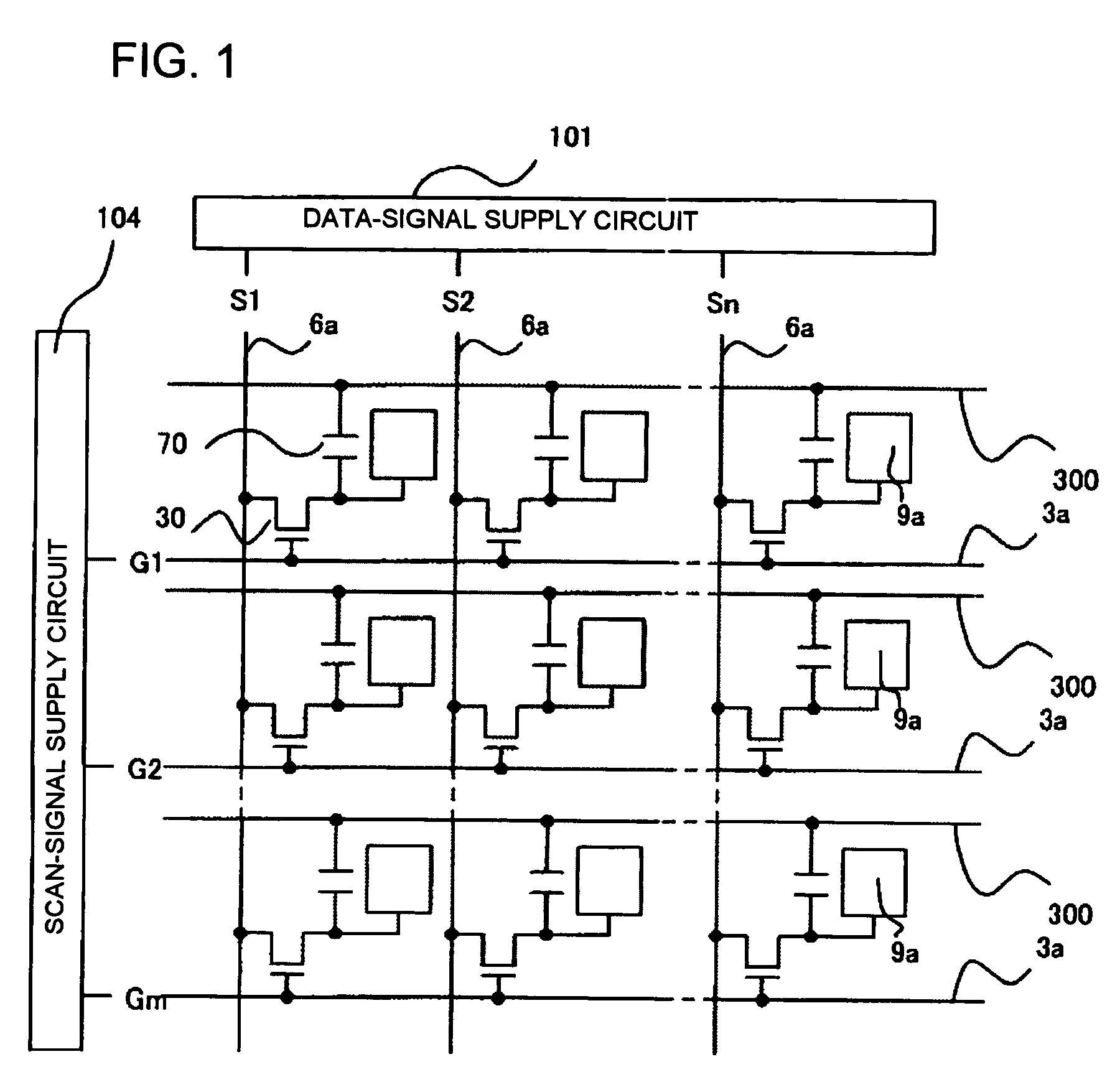
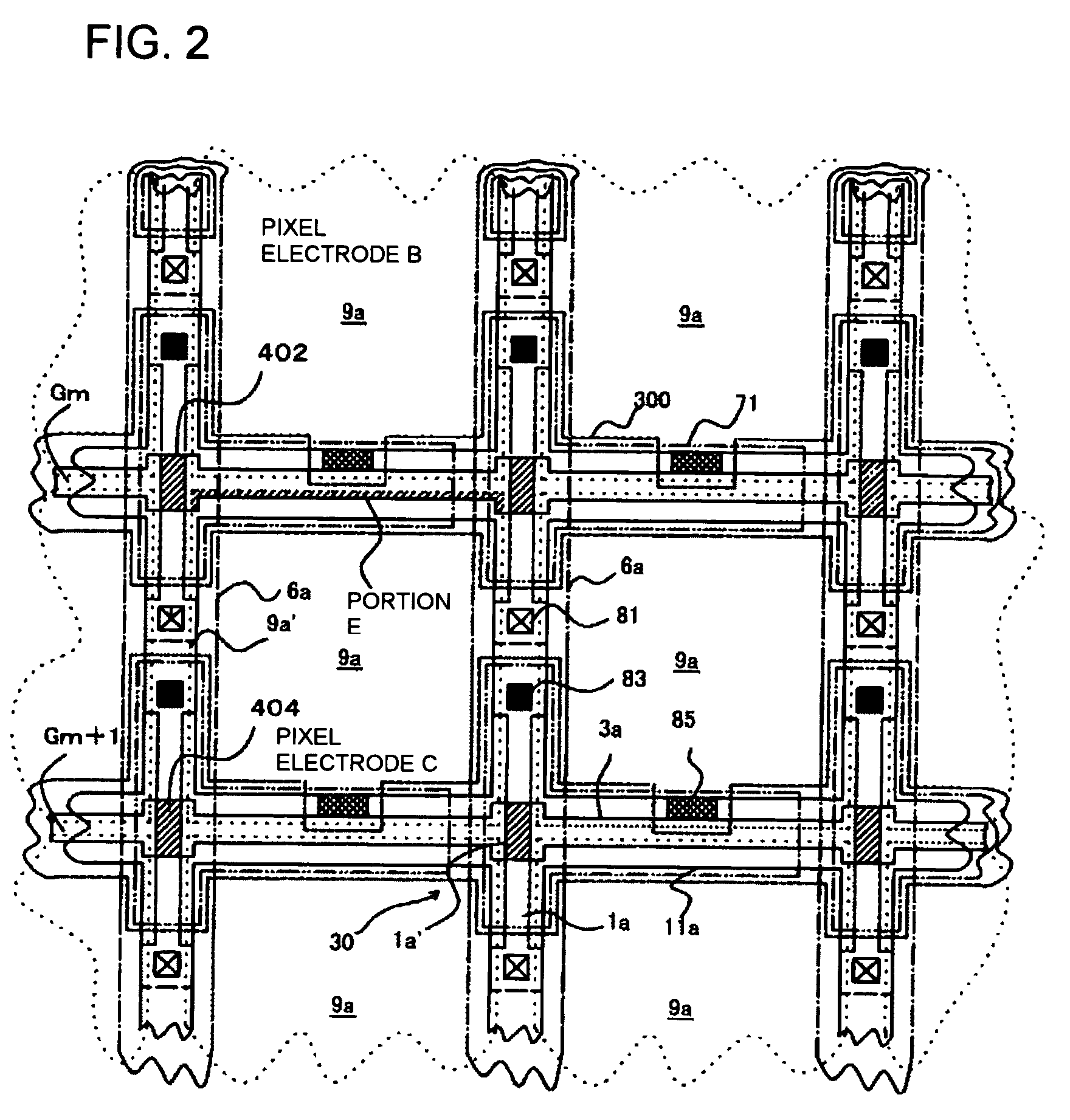
[0055]First, the basic configuration of the electro-optical device of the first exemplary embodiment is described with reference to FIGS. 1 to 3. FIG. 1 is a schematic circuit diagram showing an equivalent circuit of various elements, wires, and the like for a plurality of pixels that are formed in a matrix to constitute the image display area of the electro-optical device, in conjunction with peripheral drive circuits therefor. FIG. 2 is a plan view of a group of multiple pixels that are adjacent to each other on a TFT-array substrate on which data lines, scan lines, pixel electrodes, and the like are formed. FIG. 3 is a timing chart of a data signal, scan signals, and the like in a comparative example.

[0056]Referring to FIG. 1, the plurality of pixels, which are formed in a matrix to constitute the image display area of the electro-optical devi...

second exemplary embodiment

[0085]A second exemplary embodiment of the electro-optical device is described below with reference to FIGS. 6 and 7. FIG. 6 is a timing chart showing the timings of a data-line drive signal and scan signals in the second embodiment. FIG. 7 is a schematic showing a scan-signal supply circuit and middle-stage wave circuits that are configured to generate two types of scan signals in this exemplary embodiment.

[0086]In the second exemplary embodiment, the pixel electrodes 9a in the same row are driven by potentials having the same polarity and 1H inversion driving in which the potential polarities are inverted for each row in a field period is performed. That is, image signals supplied from the data-signal supply circuit 101 are signals whose polarities are inverted for each field unit. This can effectively prevent deterioration resulting from application of a DC voltage to the liquid crystal. The basic configuration of the electro-optical device of this second exemplary embodiment is ...


PUM


Abstract

A plurality of pixel electrodes, TFTs to control the switching of the pixel electrodes, scan lines to supply scan lines to the gates of the TFTs, and data lines to supply image signals to the pixel electrodes via the TFTs when the TFTs are put into an ON state are provided on a substrate. A scan-signal supply circuit to line-sequentially supply the scan signals is further provided. The scan-signal supply circuit holds the scan signals to an intermediate potential for a predetermined period in the middle of changing the potential of the scan signals between a high potential that puts the TFTs into the ON state and a low potential that puts the TFTs into the OFF state.

Description

BACKGROUND OF THE INVENTION[0001]1. Field of Invention[0002]The present invention relates to electro-optical devices, such as liquid crystal devices. More particularly, the present invention relates to a type of electro-optical device that has transistors to control the switching of pixel electrodes arranged in a matrix and that performs active-matrix driving by sequentially supplying scan signals to scan lines provided for corresponding pixel rows, a drive device and a drive method which are preferably used for such an electro-optical device, and an electronic apparatus having such an electro-optical device.[0003]2. Description of Related Art[0004]The electro-optical device of this type has, in an image display area on a substrate, pixel electrodes, thin-film transistors (hereinafter “TFTs”) to switch the pixel electrodes, scan lines to supply scan signals to the corresponding TFTs, data lines to supply image signals to the sources of the TFTs, storage capacitors connected to the p...

Claims


Application Information

Patent Timeline
IPC IPC(8): G02F1/03G02F1/133G09G3/20G09G3/36
CPCG09G3/3677G09G3/3614G09G2310/06G09G2320/0247G09G2320/0219G09G2320/0223G09G2320/0204G02F1/133
Inventor AOKI, TORUISHII, KENYA
Owner 138 EAST LCD ADVANCEMENTS LTD
Features
  • Generate Ideas
  • Intellectual Property
  • Life Sciences
  • Materials
  • Tech Scout
  • Unparalleled Data Quality
  • Higher Quality Content
  • 60% Fewer Hallucinations
Learn More