Adaptive voltage scaling power supply for use in a digital processing component and method of operating the same

a digital processing and power supply technology, applied in the direction of electric variable regulation, process and machine control, instruments, etc., can solve the problems of increasing propagation delay across gates, rising times, and prior art applications that do not provide any means for finely adjusting the level of vdd

Inactive Publication Date: 2006-09-12
NAT SEMICON CORP
View PDF11 Cites 16 Cited by
  • Summary
  • Abstract
  • Description
  • Claims
  • Application Information

AI Technical Summary

Benefits of technology

[0013]To address the above-discussed deficiencies of the prior art, it is a primary object of the present invention to provide an adaptive voltage power supply that finely adjusts VDD to an optimum level. According to an advantageous embodiment of the present invention, the adaptive voltage power supply comprises: 1) a first charging circuit capable of increasing a reference voltage on a charg

Problems solved by technology

Conversely, as VDD gets smaller, rise times and propagation delays across gates increase.
Unfortunately, prior art applications do not provide any means for finely adjusting the level of VDD to a wide number of clock speeds.
Thus, in the example above, if the

Method used


Image

  • Adaptive voltage scaling power supply for use in a digital processing component and method of operating the same
  • Adaptive voltage scaling power supply for use in a digital processing component and method of operating the same
  • Adaptive voltage scaling power supply for use in a digital processing component and method of operating the same

Examples


first embodiment

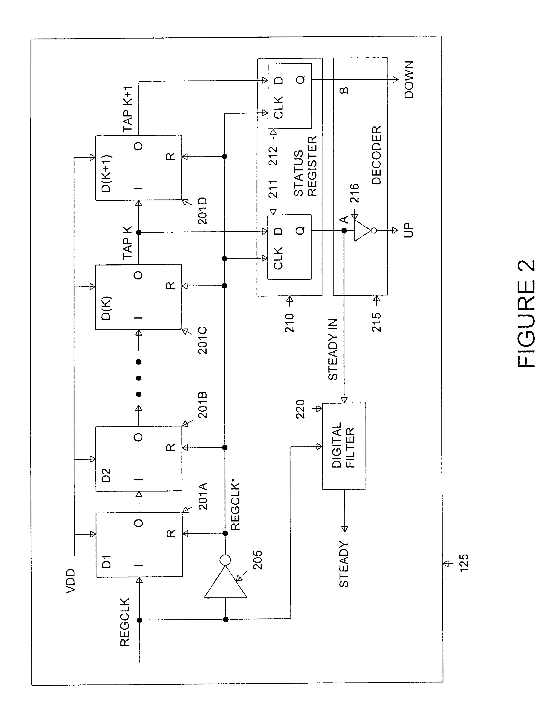
[0053]FIG. 5 illustrates AVS slack time detector 125 in greater detail according to an alternate exemplary embodiment of the present invention. AVS slack time detector 125 illustrated in FIG. 2 produced two control signals, namely UP and DOWN, which could be used to adjust the level of VDD in relatively coarse incremental steps or relatively coarse decremental steps. According to the exemplary embodiment illustrated in FIG. 5, AVS slack time detector 125 produces a plurality of control signals that may be used to increment or decrement the level of VDD by relatively small amounts and relatively large amounts.

[0054]AVS slack time detector 125 in FIG. 5 is identical in most respects to AVS slack time detector 125 illustrated in FIG. 2. The principal difference is in the number of delay cell 201 outputs that are monitored. AVS slack time detector 125 in FIG. 2 only monitored two delay cell 201 outputs (i.e., K and K+1). AVS slack time detector 125 in FIG. 5 monitors the outputs of more...

second embodiment

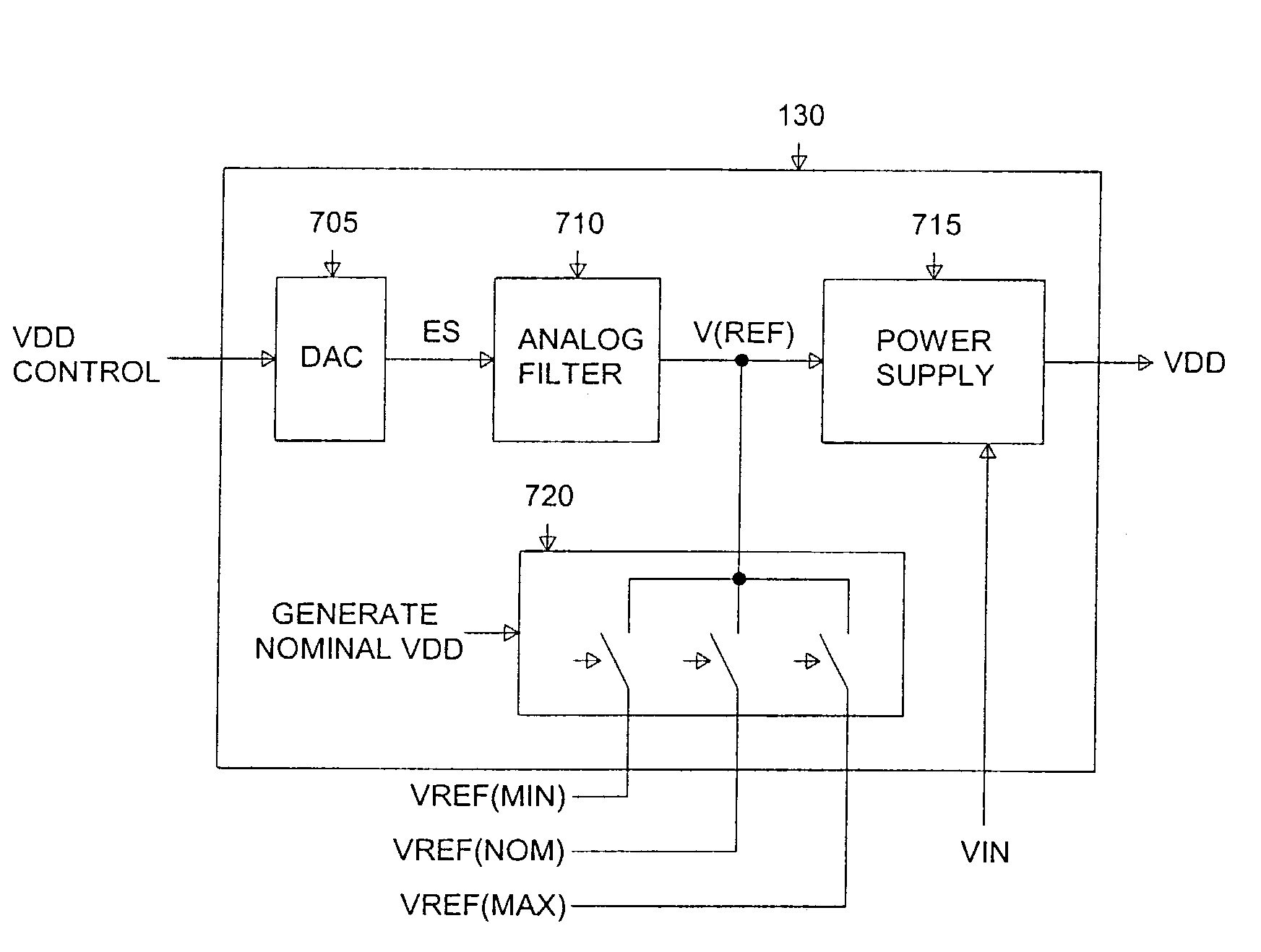
[0066]FIG. 9 illustrates digital-to-analog converter (DAC) 705 and analog filter 710 in exemplary AVS power supply 130 in greater detail according to a second exemplary embodiment of the present invention. In the second embodiment, DAC 705 comprises current source 910, current source 911, current source 930, current source 931, switch 920, switch 921, switch 940, and switch 941. Current source 910 and switch 920 form a first charging circuit that injects a current, I(PUMP), onto a relatively large capacitor, C(PUMP), in analog filter 710 whenever the VDD CONTROL signal, SMALL UP, closes switch 920. Current source 930 and switch 940 form a second charging circuit that injects current I(PUMP) onto capacitor C(PUMP) whenever the VDD CONTROL signal, LARGE UP, closes switch 940. Assuming that current sources 910 and 930 produce the same currents, the amount of current injected onto capacitor C(PUMP) can be doubled when switches 920 and 940 are closed simultaneously. Thus, a relatively fi...


PUM


Abstract

There is disclosed an adaptive voltage power supply that finely adjusts VDD to an optimum level. The adaptive voltage power supply comprises: 1) a first charging circuit capable of increasing a reference voltage on a charge capacitor in response to receipt of a first VDD control signal; 2) a second charging circuit capable of decreasing the reference voltage on the charge capacitor in response to receipt of a second VDD control signal; and 3) a power supply capable of receiving the reference voltage on the charge capacitor and generating an output power level, VDD, determined by a level of the reference voltage.

Description

[0001]This application is a continuation of prior U.S. patent application Ser. No. 10 / 053,228 filed on Jan. 19, 2002 now U.S. Pat. No. 6,548,991.CROSS-REFERENCE TO RELATED APPLICATIONS[0002]The present invention is related to those disclosed in the following U.S. patent applications:[0003]Serial No. 10 / 053,226, filed concurrently herewith, entitled “AN ADAPTIVE VOLTAGE SCALING DIGITAL PROCESSING COMPONENT AND METHOD OF OPERATING THE SAME;”[0004]Serial No. 10 / 053,227, filed concurrently herewith, entitled “ADAPTIVE VOLTAGE SCALING CLOCK GENERATOR FOR USE IN A DIGITAL PROCESSING COMPONENT AND METHOD OF OPERATING THE SAME;” and[0005]Serial No. 10 / 053,858, filed concurrently herewith, entitled “SYSTEM FOR ADJUSTING A POWER SUPPLY LEVEL OF A DIGITAL PROCESSING COMPONENT AND METHOD OF OPERATING THE SAME.”[0006]The above applications are commonly assigned to the assignee of the present invention. The disclosures of these related patent applications are hereby incorporated by reference for ...

Claims


Application Information

Patent Timeline
IPC IPC(8): G05F3/16G05F1/613
CPCG05F1/613
Inventor MAKSIMOVIC, DRAGANDHAR, SANDEEPAMBATIPUDI, RAVINDRAKRANZEN, BRUNO
Owner NAT SEMICON CORP
Why Eureka
Try Eureka