Method and apparatus for controlling an active matrix display

a technology of active matrix and display, applied in the field of displays, can solve the problems of difficult to maintain uniformity during the lifetime of the display containing an array of such pixels, difficult to produce uniform pixels, complex circuit schemes, etc., and achieve the effect of constant emission

Active Publication Date: 2006-09-12
SILICONFILE TECH INC
View PDF7 Cites 248 Cited by
  • Summary
  • Abstract
  • Description
  • Claims
  • Application Information

AI Technical Summary

Problems solved by technology

It is difficult to produce uniform pixels and even if such uniform pixels could be produced it is difficult to maintain uniformity during the lifetime of a display containing an array of such pixels.
These circuit schemes are complex, expensive to produce and have not been entirely satisfactory.
Further, the circuit elements themselves, including the photodiode all introduce variables, which introduce non-uniformity.
Further this approach only tends to cause uniformity since bright pixels are shut down faster and dim pixels are left on longer, but no exact brightness level is measured or used as a reference.
Another problem is that the particular feedback circuit and method can set the system into oscillations, which if not damped within the line write time, would leave the actual brightness and voltage undetermined at the point of write time cut off.

Method used


Image

  • Method and apparatus for controlling an active matrix display
  • Method and apparatus for controlling an active matrix display
  • Method and apparatus for controlling an active matrix display

Examples


Embodiment Construction

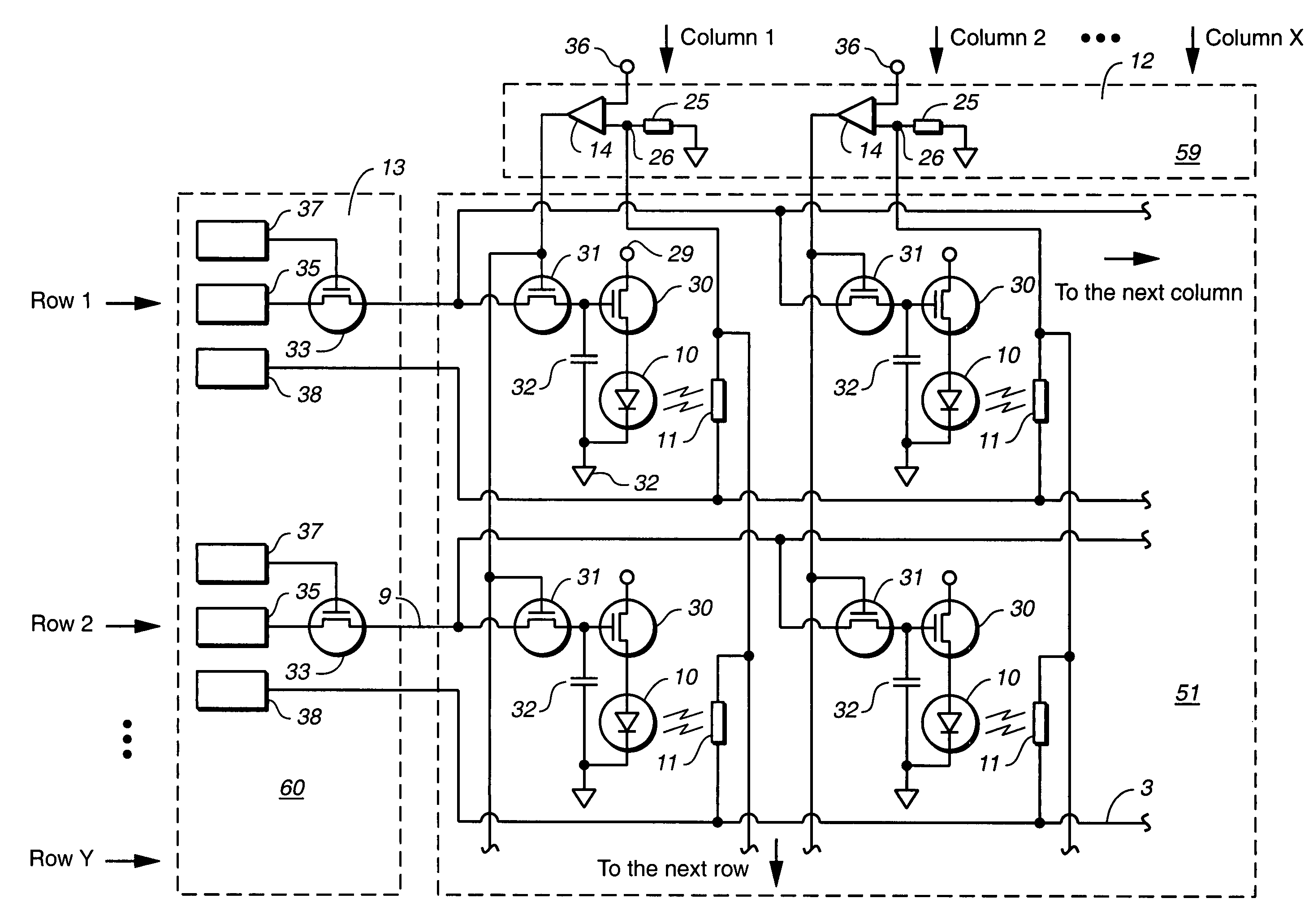
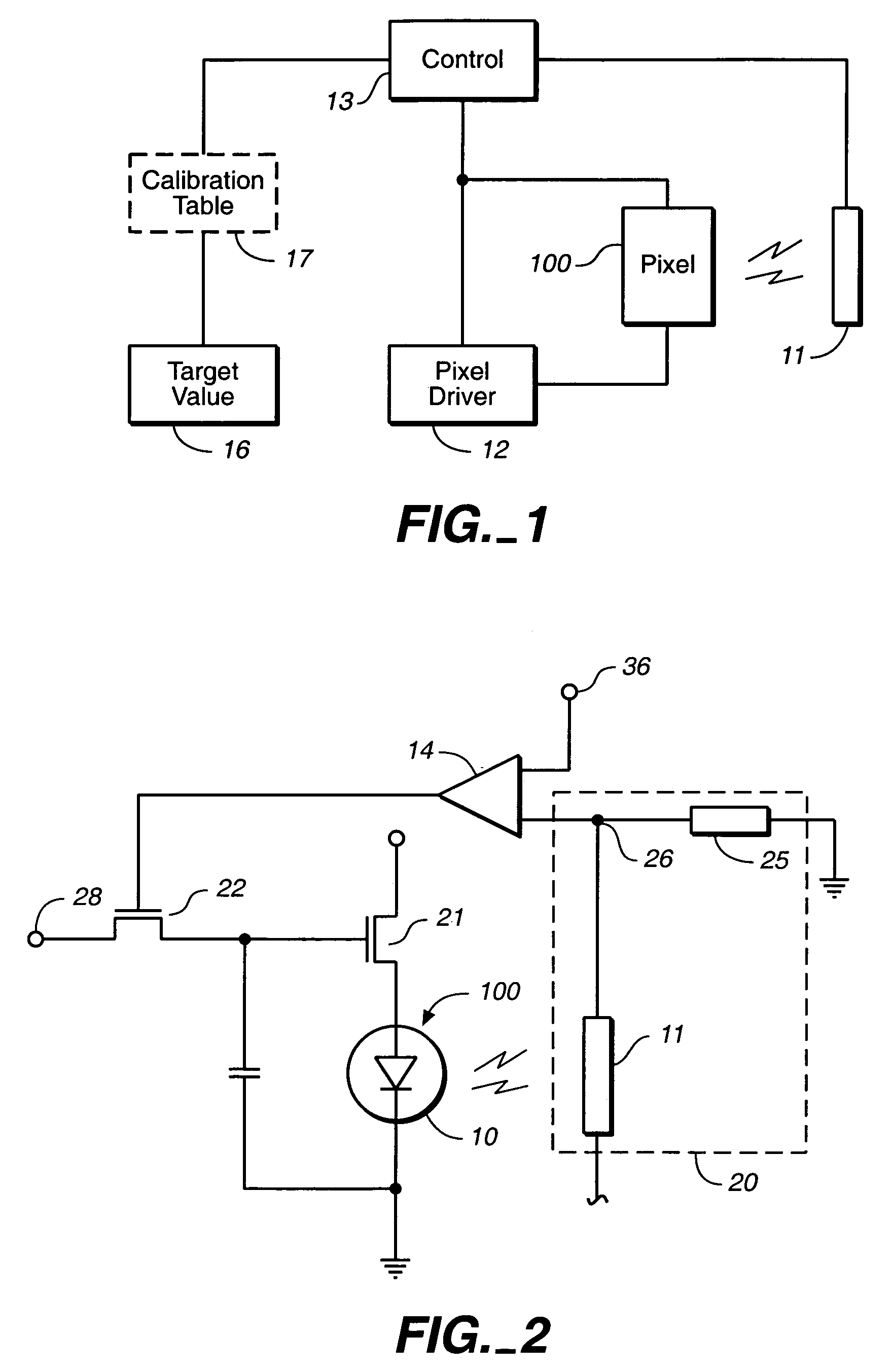
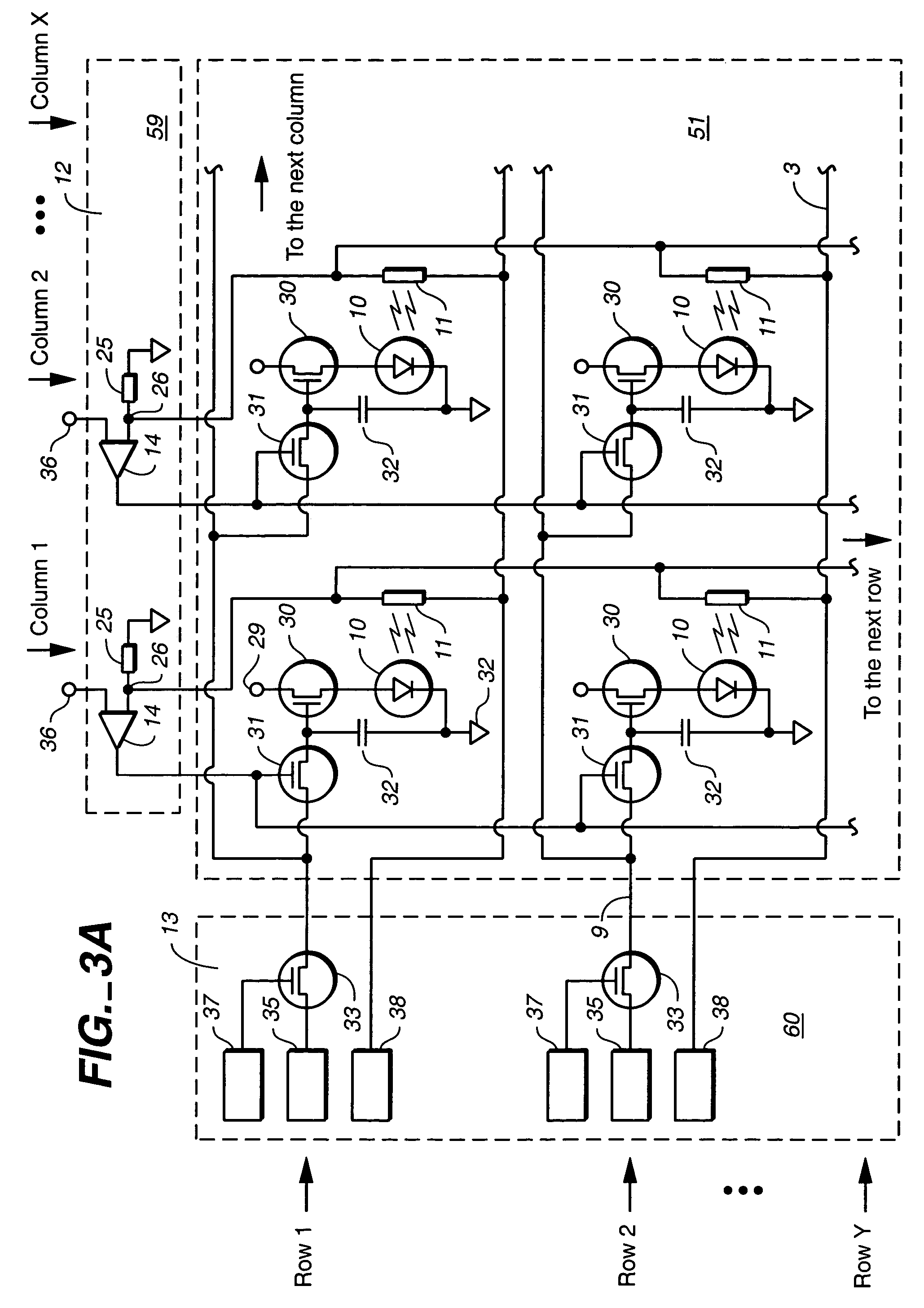
[0020]Embodiments of the present invention provide systems, methods, circuits, and apparatuses for controlling emission from a pixel. The emission source may be generally any source known in the art that produces radiation in response to a supplied voltage—including light emitting diodes and organic light emitting diodes at any wavelength including white organic light emitting diodes. In some embodiments, such as an LCD display, the light source is a backlight and light emission from the pixel is controlled by varying the amount of light from the backlight passed through the pixel. Other light sources may be used including electroluminescent cells, inorganic light emitting diodes, vacuum florescent displays, field emission displays and plasma displays. While radiation (or illumination) sources intended to display graphics, images, text, or other data or information for human viewing will primarily be in the visual wavelengths (generally about 400–700 nanometers) it is understood tha...


PUM


Abstract

A method of controlling an array of pixels in an active matrix display to a predetermined emission level is provided. The pixels are arranged in a plurality of rows and a plurality of columns, each pixel having an active matrix element. The method makes use of a plurality of sensors each having a measurable sensor parameter and at least one pixel driver. Light emission is varied from a plurality of pixels in a first row using the pixel driver and the active matrix elements in the pixels. Light emission is received from the pixels at the sensors and a measured value of the measurable sensor parameter is obtained responsive to the received light emission. For each of the plurality of pixels, a control signal is generated for the pixel to maintain constant emission from the light source at the predetermined emission level.

Description

CROSS-REFERENCE TO RELATED APPLICATIONS[0001]The present application claims the benefit of the filing date under 35 U.S.C. §119(e) of U.S. Provisional Application Ser. No. 60 / 479,342 filed 18 Jun. 2003 entitled “Emission Feedback Stabilized Flat Panel Display”, U.S. Provisional Application Ser. No. 60 / 523,396 filed 19 Nov. 2003 entitled “Passive Matrix Emission Stabilized Flat Panel Display”, and U.S. Provisional Application Ser. No. 60 / 532,034, filed 22 Dec. 2003, entitled “Stabilized Flat Panel Display”, all of which are incorporated herein by reference in their entirety.[0002]The present application is a continuation-in-part of U.S. patent application Ser. No. 10 / 841,198 filed May 6, 2004 entitled “Method and Apparatus for Controlling Pixel Emission,” incorporated herein by reference.TECHNICAL FIELD[0003]The present invention relates generally to displays, and more particularly, to control of the gray-level or color and brightness of active matrix displays and picture elements of...

Claims


Application Information

Patent Timeline
Patent Type & Authority Patents(United States)
IPC IPC(8): G09G3/36G09G3/32G09G3/34
CPCG09G3/3233G09G3/3291G09G2360/148G09G3/3426G09G2300/0819G09G2300/0842G09G2310/0259G09G2310/027G09G2310/066G09G2320/0233G09G2320/0285G09G2320/0295G09G2320/043G09G2320/045G09G2320/0626G09G2330/021G09G2360/147G09G3/20G09G3/30G09G3/32G09G3/36
Inventor NAUGLER, W. EDWARD
Owner SILICONFILE TECH INC
Why Eureka
Try Eureka