System and method for reducing wire delay or congestion during synthesis of hardware solvers

a hardware solver and delay technology, applied in the field of computer systems, can solve the problems of delay of any register to register path, inability to know the delay of wires, and time-consuming processing of nested loop codes

Active Publication Date: 2006-09-12
SAMSUNG ELECTRONICS CO LTD
View PDF18 Cites 81 Cited by
  • Summary
  • Abstract
  • Description
  • Claims
  • Application Information

AI Technical Summary

Problems solved by technology

Nested loop code can be very time consuming to process, as inner loops must be processed repeatedly for each increment of an outer loop.
This means that the delay of any register to register path must be within the clock period.
The problem is that the wire delay will not be known until after the backend physical design process.
The problem is that there is a large variability of wire delay from circuit to circuit.
Predicting this can be difficult since the delay of each wire depends on the placement of components and the contention for routing resources during backend physical design.
This method is expensive in design time since backend physical design is a very time consuming process.
The drawback of this method is that many hardware solvers will be over-designed since too much slack will have been provided.
This may result in an area inflated hardware solver since more registers will have been created than necessary.
Routing congestion is another problem encountered during backend physical design.
Routing congestion is the interference of signals as they compete for routing resources.
Routing congestion is bad because it can often affect area, timing, and / or power consumption.
Designs often have constraints in one or more of these areas, and RTL causing too much routing congestion can cause one or more of the requirements to not be met (e.g. area, timing, power, etc).
The routing congestion problem may be different for difficult backend target technologies.
The problem is that if the netlist is too connected, many functions will need to be placed very close together with lots of communication between them.
However, there might not be enough routing resources to place these functions close together since there is a fixed amount of routing resources per unit area on the FPGA.
Placing these close exhausts all of the routing resources.
But that 1) makes timing harder because the communications must now travel further, and 2) increases area since the functions are physically spaced further apart.
However, adding buffers to the circuit is expensive in terms of area and power.
Retiming moves existing registers within the circuit to other locations, such as nets in which wire delay is a problem.
However, retiming is often not used because of the difficulty of moving registers with initial values across devices (such as multipliers), since determining the new value requires inverting the function of the device—often an impossible task.
In addition, retiming is limited since registers cannot be added (or subtracted) to cycles in the circuit.
Hence, if a path with a wire delay problem is part of a cycle and requires more registers to compensate for the wire delay than available around the cycle, retiming will not help.
However, pipelining is often not used since increasing latency changes the circuit's I / O behavior and may not be acceptable for certain designs.

Method used


Image

  • System and method for reducing wire delay or congestion during synthesis of hardware solvers
  • System and method for reducing wire delay or congestion during synthesis of hardware solvers
  • System and method for reducing wire delay or congestion during synthesis of hardware solvers

Examples


Embodiment Construction

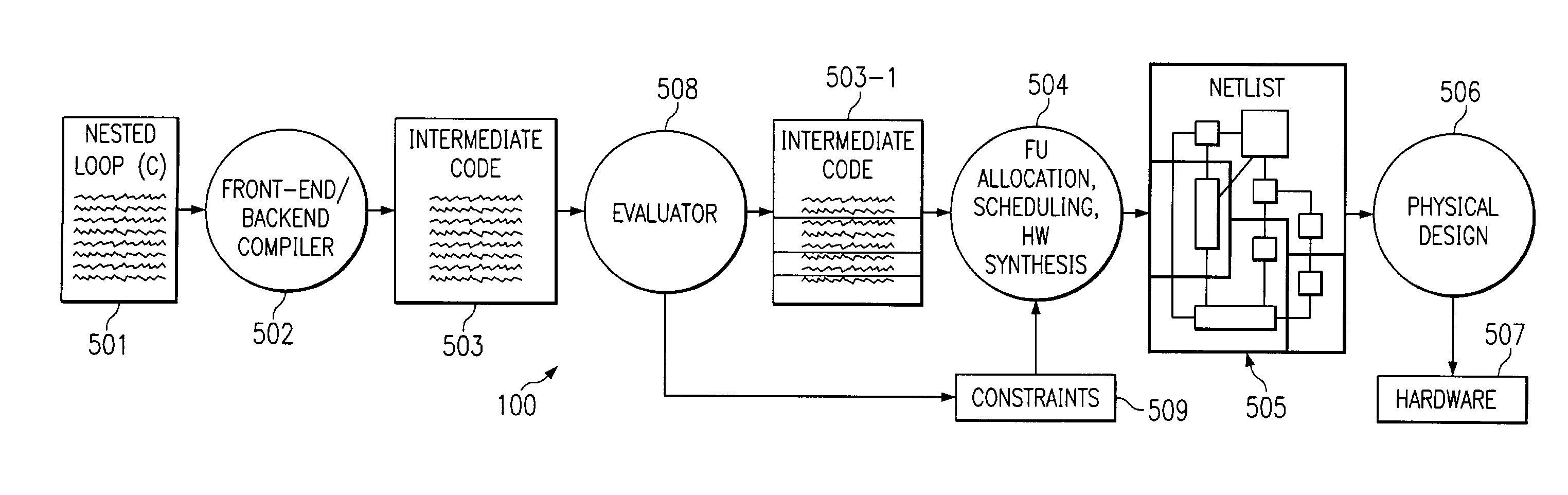
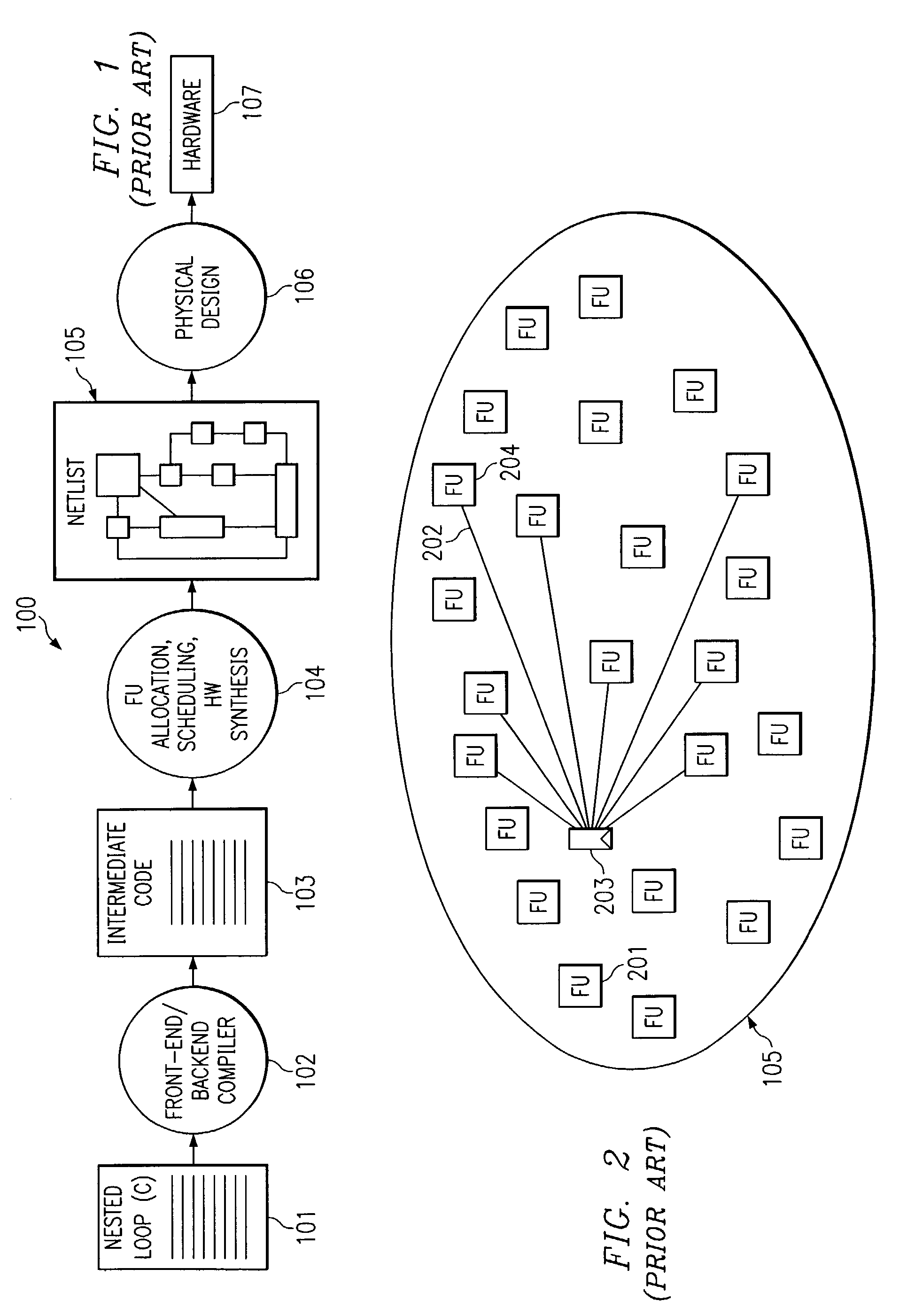
[0032]An embodiment of the invention is a method for handling routing delay and / or congestion during the automatic synthesis of hardware solvers prior to backend physical design. An embodiment of the invention modifies high-level synthesis to generate a netlist for the logical device that is more amenable to successful physical design and reduces wire delay and / or congestion. Successful physical design involves meeting area and timing requirements within a target technology, such as FPGAs or standard cells. Existing design automation methods handle wire delay by over-designing the hardware solver in order to leave room for wire delay. The amount of the clock period that is left “on the table” for wire delay is called the wiring slack, routing slack, or just slack. The problem is that there is a large variability of wire delay from circuit to circuit, and predicting this can be difficult since the delay of each wire depends on the placement of components and the contention for routin...


PUM


Abstract

One embodiment of the invention is a method for producing a hardware solver for intermediate code comprising analyzing intermediate code for at least one instantiation that may cause at least one of wire delay and congestion in the solver, forming compensation for the at least one instantiation, and forming the solver in accordance with the compensation.

Description

FIELD OF THE INVENTION[0001]This invention relates in general to computer systems and in specific to a system and method for reducing wire delay and / or congestion in hardware solvers.DESCRIPTION OF THE RELATED ART[0002]Design automation is the process of taking a computer program, written in a high-level language, such as C, and producing a hardware circuit with the same functionality as the computer program. In other words, code from a program is converted into compute devices (such multipliers and adders) to perform the program's computation, memory devices (such as registers and RAM) to store the program's data, and control devices (such as finite-state-machines and microcontrollers) to execute the program's instructions. The hardware circuit resulting from design automation is specified at the register-transfer-level (RTL), which is a cycle-level structural description of the all of the hardware. Once this “C-to-RTL” automation is complete, physical design maps the RTL onto a ph...

Claims


Application Information

Patent Timeline
Patent Type & Authority Patents(United States)
IPC IPC(8): G06F17/50G06F9/45
CPCG06F17/5072G06F17/5045G06F30/392G06F30/30
Inventor CRONQUIST, DARREN C.
Owner SAMSUNG ELECTRONICS CO LTD
Why Eureka
Try Eureka