Optimal operation of conformal silica deposition reactors

Active Publication Date: 2006-09-19
NOVELLUS SYSTEMS
View PDF44 Cites 66 Cited by
  • Summary
  • Abstract
  • Description
  • Claims
  • Application Information

AI Technical Summary

Benefits of technology

[0008]The present invention meets these needs by providing methods of forming conformal films that reduce the amount of metal-containing and/or silicon containing precursor materials required. The methods of the present invention increase the amount of film grown following each dose of metal-containing precursor. In some embodiments, the methods of the present invention increa

Problems solved by technology

However, as design rules continue to shrink, the aspect ratios (depth to width) of features increase, and traditional CVD techniques can no longer provide adequately conformal films in these high aspect ratio features.
Thus, in conventional RVD (and ALD) reactors, a significant amount of the silicon-containing precu

Method used


Image

  • Optimal operation of conformal silica deposition reactors
  • Optimal operation of conformal silica deposition reactors
  • Optimal operation of conformal silica deposition reactors

Examples


Embodiment Construction

[0027]In the following detailed description of the present invention, numerous specific embodiments are set forth in order to provide a thorough understanding of the invention. However, as will be apparent to those skilled in the art, the present invention may be practiced without these specific details or by using alternate elements or processes. In other instances well-known processes, procedures and components have not been described in detail so as not to unnecessarily obscure aspects of the present invention.

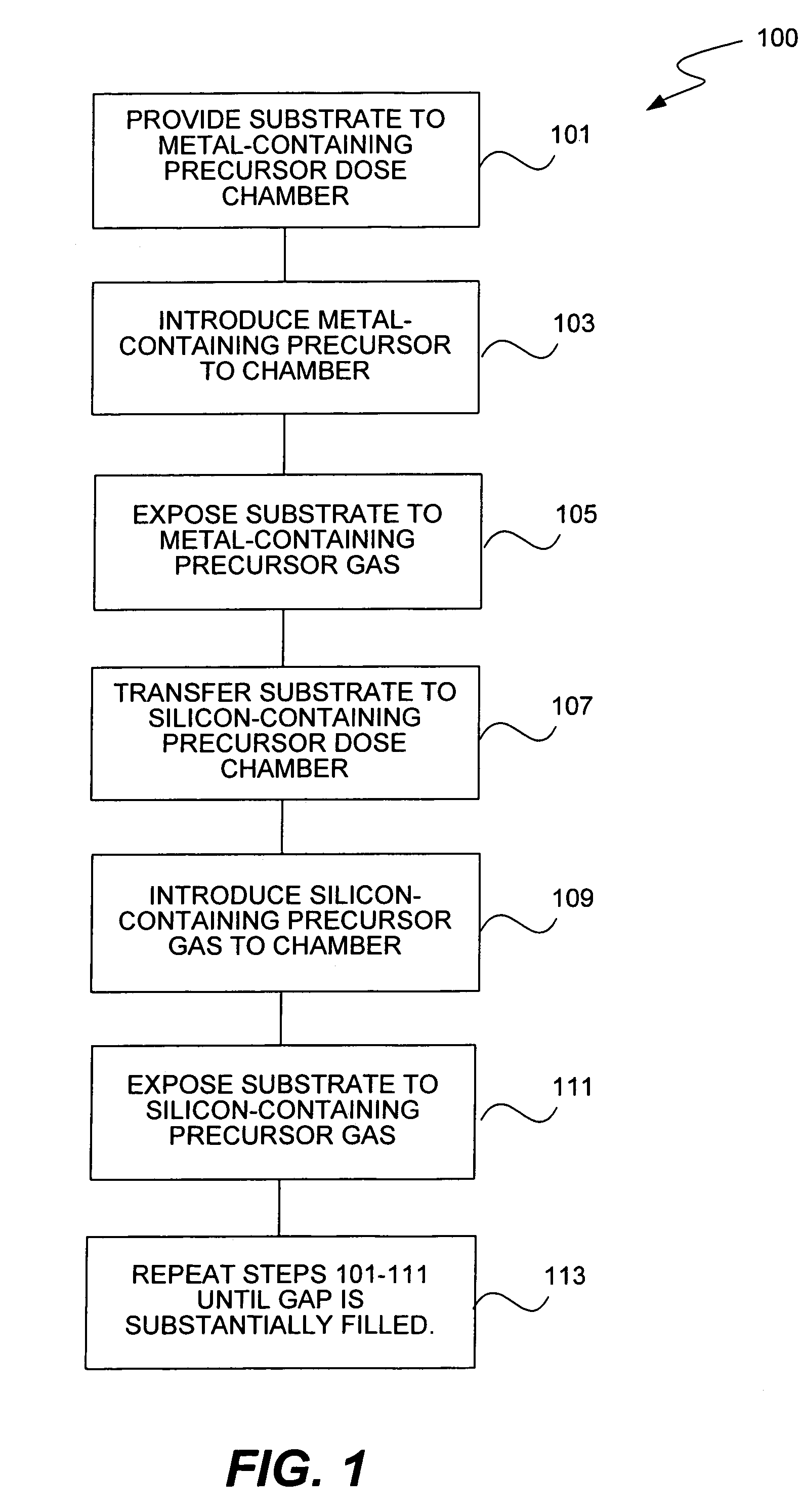
[0028]As indicated, the present invention provides methods of forming conformal films with increased efficiency. The methods may be used with conformal film deposition techniques such as RVD and ALD. The methods are particularly suited for used with RVD.

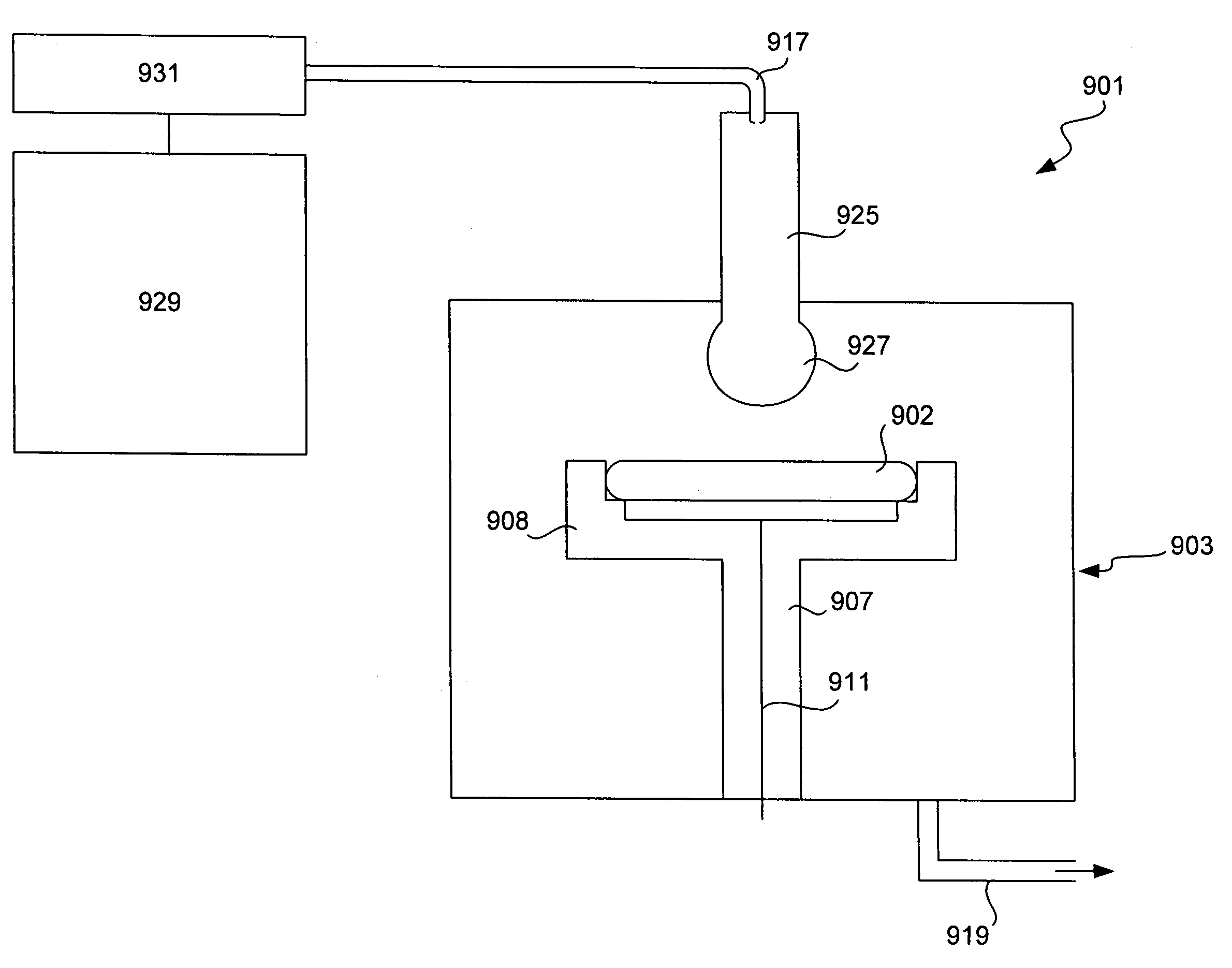
[0029]Generally, conventional RVD methods involve sequentially depositing a plurality of atomic-scale films on a substrate surface by sequentially exposing and removing reactants to and from the substrate surface. First, a m...


PUM

PropertyMeasurementUnit
Temperatureaaaaaaaaaa

Abstract

Methods of forming conformal films that reduce the amount of metal-containing precursor and/or silicon containing precursor materials required are described. The methods increase the amount of film grown following each dose of metal-containing and/or silicon-containing precursors. The methods may involve introducing multiple doses of the silicon-containing precursor for each dose of the metal-containing precursor and/or re-pressurizing the process chamber during exposure to a dose of the silicon-containing precursor. The methods of the present invention are particularly suitable for use in RVD processes.

Description

CROSS-REFERENCE TO RELATED APPLICATION[0001]This application is related to U.S. patent application Ser. No. 11 / 077,198, filed Mar. 9, 2005.FIELD OF THE INVENTION[0002]This invention pertains to methods for forming high density, conformal, silica nanolaminate films. More specifically, the invention pertains to methods of depositing a conformal film of dielectric material on semiconductor substrates and in structures of confined geometry such as high aspect ratio gaps.BACKGROUND OF THE INVENTION[0003]Layers of dielectric film are used in several applications in sub-micron integrated circuits (ICs) fabrication. Four such applications are shallow trench isolation (STI), premetal dielectric (PMD), inter-metal dielectric (IMD) and interlayer dielectric (ILD). All four of these layers require silicon dioxide films that fill features of various sizes and have uniform film thicknesses across the wafer.[0004]Chemical vapor deposition (CVD) has traditionally been the method of choice for depos...

Claims


Application Information

Patent Timeline
IPC IPC(8): H01L21/31
CPCC23C16/402C23C16/45523C23C16/45527C23C16/45551C23C16/45557H01L21/02216H01L21/0228H01L21/31612H01L21/31625H01L21/31629H01L21/02164Y10S438/909
Inventor PAPASOULIOTIS, GEORGE D.
Owner NOVELLUS SYSTEMS
Why Eureka
Try Eureka