Device and method for fabrication of microchannel plates using a mega-boule wafer

a mega-boule wafer and micro-channel plate technology, applied in the field of micro-channel plate, can solve the problem of large touch labor for a part that is very sensitiv

Inactive Publication Date: 2006-09-19
EXCELIS INC
View PDF4 Cites 4 Cited by
  • Summary
  • Abstract
  • Description
  • Claims
  • Application Information

AI Technical Summary

Benefits of technology

[0059]Advantages of the present invention are many. The shape and size of the monolithic stack may depend on the type of semiconductor wafer fabrication tools available. The shape and size of the mega-boule wafer, which is diced from the monolithic stack, may also depend on the type of semiconductor wafer fabrication tools are available. Consequently, specialized tools may be avoided.

Problems solved by technology

Handling each boule wafer individually leads to large amounts of touch labor for a part very sensitive to particle contamination.

Method used


Image

  • Device and method for fabrication of microchannel plates using a mega-boule wafer
  • Device and method for fabrication of microchannel plates using a mega-boule wafer
  • Device and method for fabrication of microchannel plates using a mega-boule wafer

Examples


Embodiment Construction

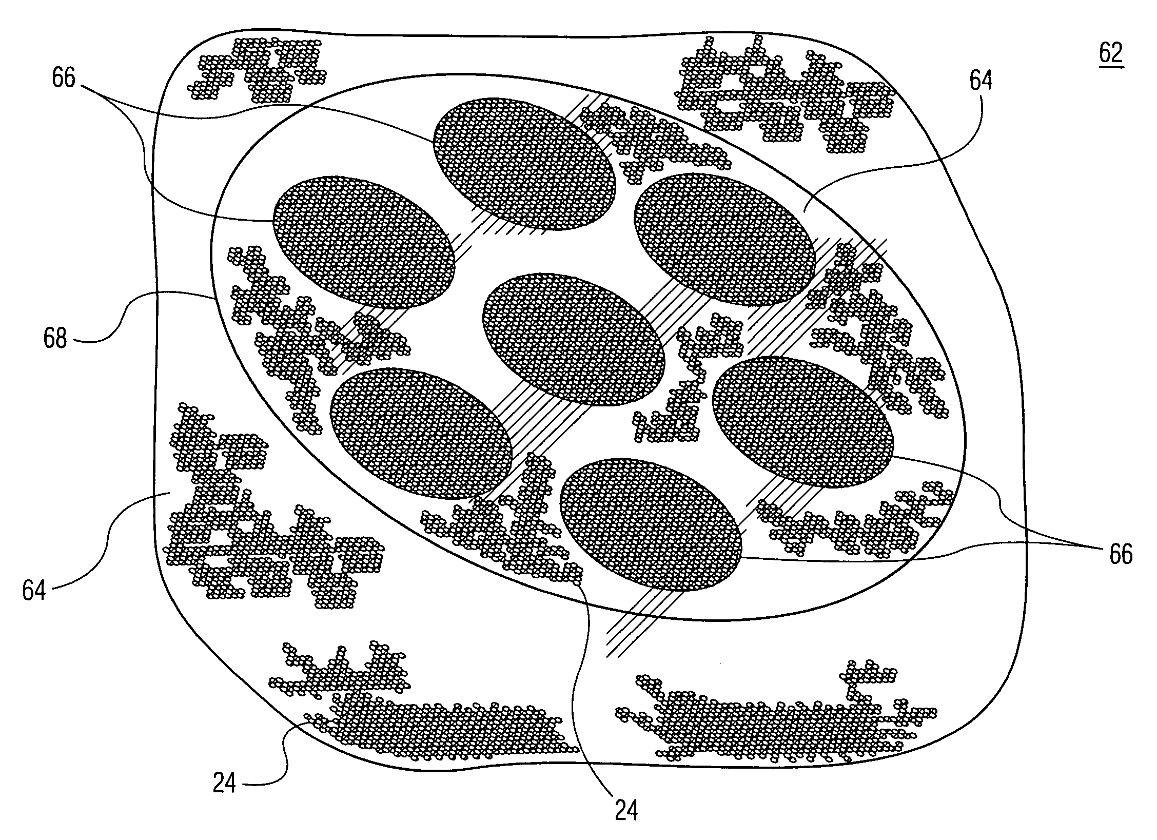
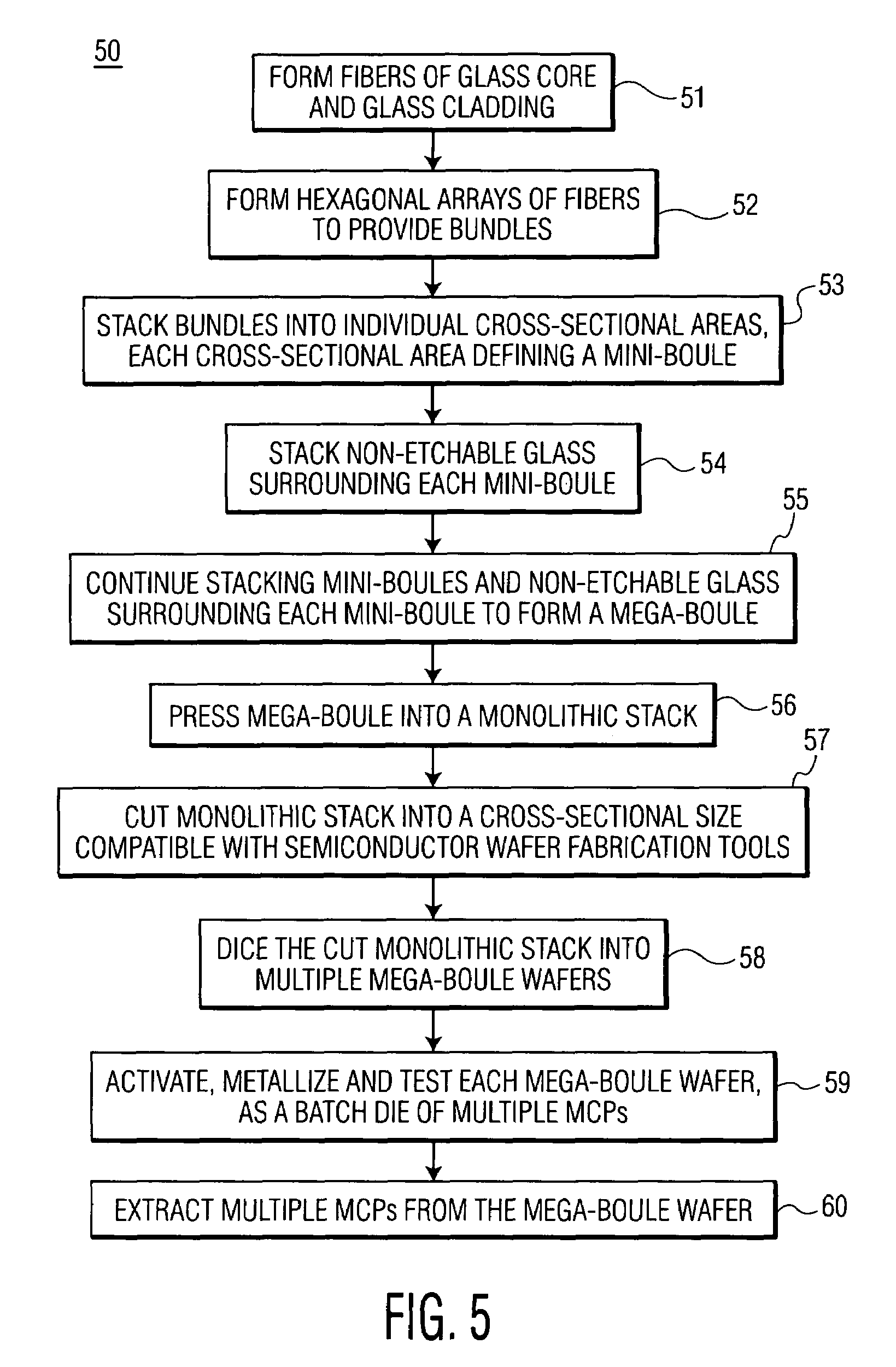
[0036]The present invention relates to forming a plurality of MCPs by using a method amenable to conventional wafer fabrication tools. More specifically, an embodiment of a method of the present invention is shown in FIG. 5, and is generally designated by reference numeral 50. As will be explained, the method forms a batch die for making multiple MCPs from a single large wafer. The single large wafer, referred to as a mega-boule wafer, is sized to be accommodated by conventional wafer fabrication tools.

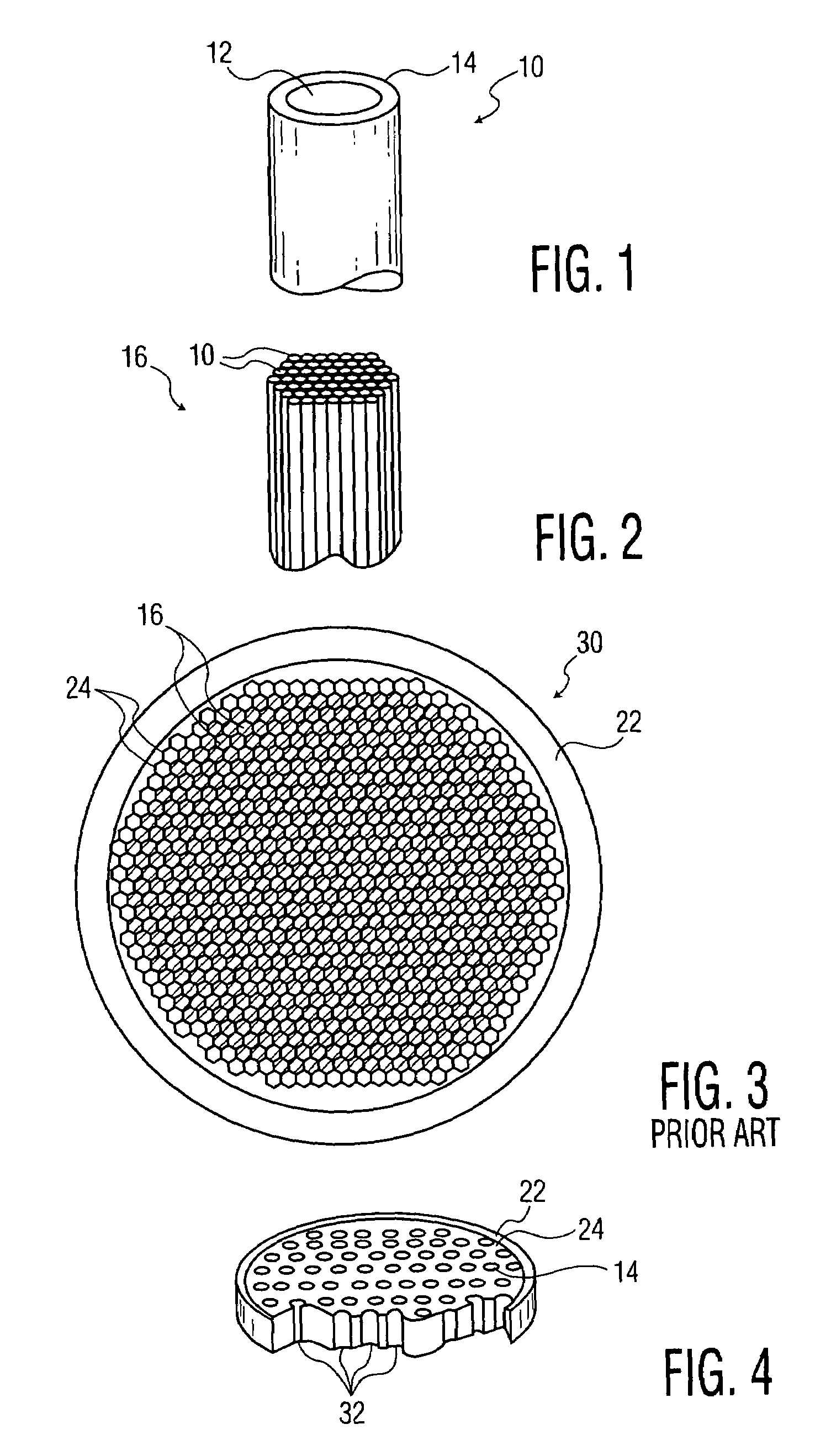
[0037]Referring now to FIG. 5 and beginning with step 51, fibers of glass core and glass cladding are formed by method 50. Starting fiber 10 is shown in FIG. 1 and includes glass core 12 and glass cladding 14. Core 12 is made of material that is etchable, so that the core may be subsequently removed by etching a mega-boule wafer, in accordance with the present invention. Glass cladding 14 is made of glass that is non-etchable under the same conditions that allow etching of core 12. Th...


PUM


Abstract

The present invention provides a mega-boule for use in fabricating microchannel plates (MCPs). The mega-boule includes a cross-sectional surface having at least first, second and third areas, each area occupying a distinct portion of the cross-sectional surface. The first and second areas include a plurality of optical fibers, transversely oriented to the cross-sectional surface, each optical fiber having a cladding formed of non-etchable material and a core formed of etchable material. The third area is disposed interstitially between and surrounding the first and second areas, and includes non-etchable material.

Description

TECHNICAL FIELD[0001]The present invention relates to microchannel plates (MCPs) for use with image intensifiers, and more specifically, to a device and method for fabrication of multiple MCPs using a mega-boule wafer.BACKGROUND OF THE INVENTION[0002]Microchannel plates are used as electron multipliers in image intensifiers. They are thin glass plates having an array of channels extending there through and are located between a photocathode and a phosphor screen. An incoming electron from the photocathode enters the input side of the microchannel plate and strikes a channel wall. When voltage is applied across the microchannel plate, these incoming or primary electrons are amplified, generating secondary electrons. The secondary electrons then exit the channel at the back end of the micrcochannel plate and are used to generate an image on the phosphor screen.[0003]In general, fabrication of a microchannel plate starts with a fiber drawing process, as disclosed in U.S. Pat. No. 4,912...

Claims


Application Information

Patent Timeline
Patent Type & Authority Patents(United States)
IPC IPC(8): H01J43/00H01J9/12H01J43/24
CPCH01J43/246H01J9/125
Inventor SMITH, ARLYNN WALTERVRESCAK, WARREN D.DEVOE, NELSON CHRISTOPHERROSINE, STEVE DAVIDSMITH, WILLIAM ALLEN
Owner EXCELIS INC
Why Eureka
Try Eureka