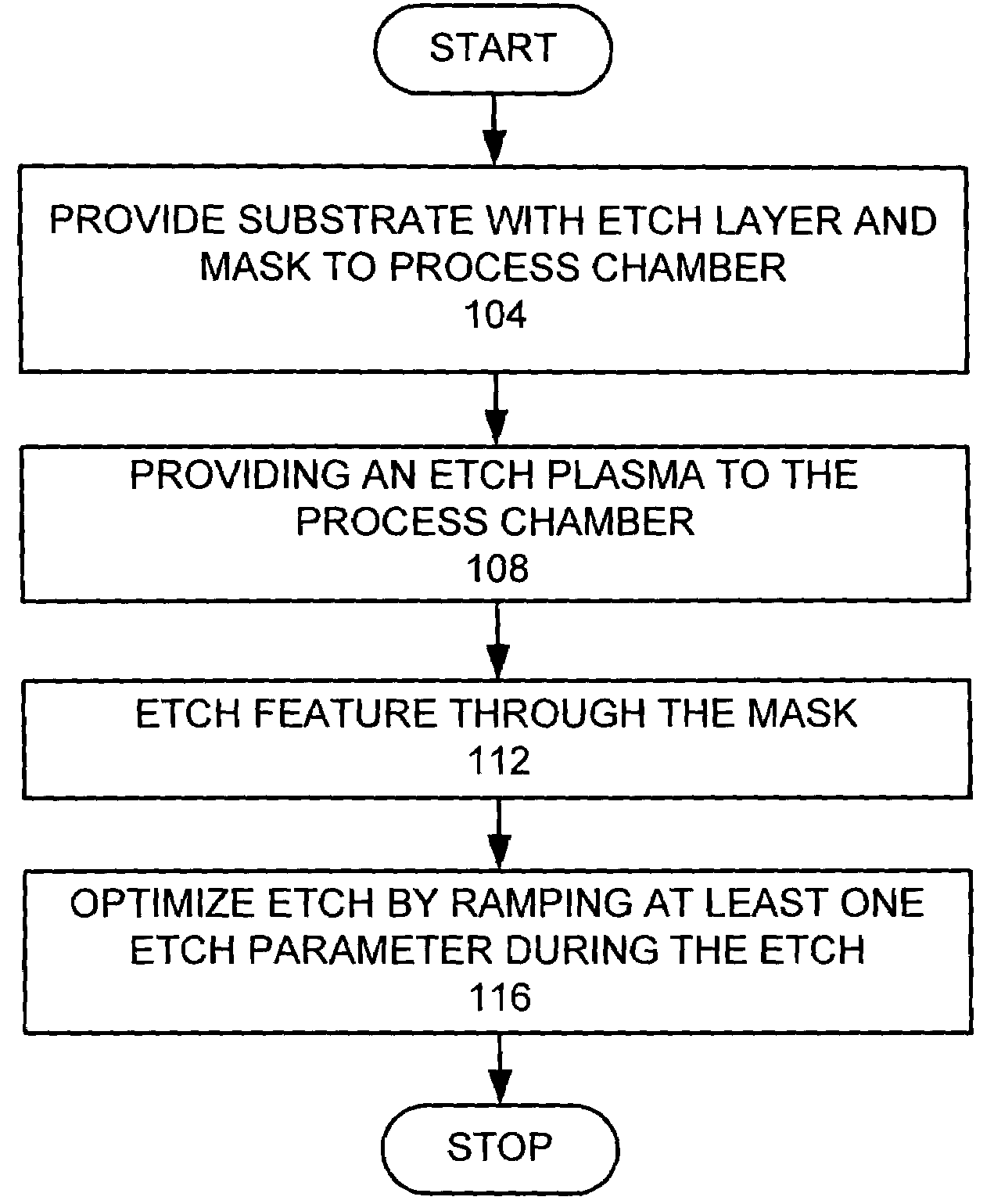
Etch with ramping

a technology of etching and ramping, which is applied in the direction of basic electric elements, electrical equipment, electric discharge tubes, etc., can solve the problems that the dielectric layer formed of siosub>2 /sub>may not effectively insulate the conductive lines, and the critical dimension of the opening may be limited by the thickness of the mask

Inactive Publication Date: 2006-11-14
LAM RES CORP
View PDF12 Cites 12 Cited by
  • Summary
  • Abstract
  • Description
  • Claims
  • Application Information

AI Technical Summary

Benefits of technology

[0009]To achieve the foregoing and in accordance with the purpose of the present invention a method for etching a feature in an etch layer through a mask over a substrate. The substrate is placed in a process chamber. An etch plasma is provided to the process chamber, where the etch plasma begins to etch. A feature is etched in the etch layer with the etch plasma. At least one etch plasma parameter is ramped during the etching of the feature to optimize plasma parameters to the changing etch depth and the feature is etched with the ramped plasma until the feature is etched to a feature depth.

Problems solved by technology

As a consequence of the increasing line densities and operating frequencies in semiconductor devices, dielectric layers formed of SiO2 may not effectively insulate the conductive lines to the extent required to avoid increased coupling capacitance levels.
If a thick mask is required to allow the etching of a high-aspect ratio opening, the critical dimension of the opening may be limited by the thickness of the mask.

Method used


Image

  • Etch with ramping
  • Etch with ramping
  • Etch with ramping

Examples


examples

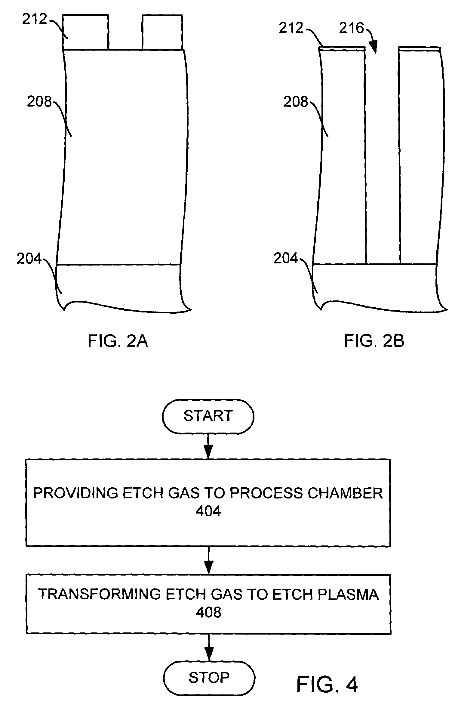
[0043]In an example of the invention, the substrate is a silicon substrate, the etch layer is a silicon oxide dielectric layer, and the mask is a photoresist mask.

[0044]Baseline Main Etch

[0045]A baseline main etch of the dielectric layer is performed in the above mentioned Exelan using the following recipe. The process chamber pressure was set to about 45 millitorr. The 27 MHz RF source provided about 1500 Watts of power to the lower electrode. The 2 MHz RF source provided about 1500 Watts of power to the lower electrode. A flow of about 300 sccm Ar, 30 sccm C4F8, and 10 sccm O2 forming an etch gas was provided. A helium cooling pressure, to cool the substrate, was 20 Torr. The lower electrode was maintained at 0° C. The upper electrode was maintained at 140° C. The baseline etch was carried out for about 250 seconds.

[0046]First Ramp Test Main Etch

[0047]A first ramp test main etch comprised a five step process with the following recipe. In each step, the process chamber pressure was...


PUM

PropertyMeasurementUnit
time periodaaaaaaaaaa
dielectric constantaaaaaaaaaa

Abstract

A method for etching a feature in an etch layer through a mask over a substrate. The substrate is placed in a process chamber. An etch plasma is provided to the process chamber, where the etch plasma begins to etch. A feature is etched in the etch layer with the etch plasma. At least one etch plasma parameter is ramped during the etching of the feature to optimize plasma parameters with the changing etch depth and the feature is etched with the ramped plasma until the feature is etched to a feature depth.

Description

BACKGROUND OF THE INVENTION[0001]The present invention relates to plasma etching. More particularly, the present invention relates to plasma etching to form deep openings with high aspect ratios such as, but not limited to, high-aspect ratio contacts (HARC).[0002]During semiconductor wafer processing, features of the semiconductor device are defined in the wafer using well-known patterning and etching processes. In these processes, a photoresist (PR) material may be deposited on the wafer and then is exposed to light filtered by a reticle. The reticle is generally a glass plate that is patterned with exemplary feature geometries that block light from propagating through the reticle.[0003]After passing through the reticle, the light contacts the surface of the photoresist material. The light changes the chemical composition of the photoresist material such that a developer can remove a portion of the photoresist material. In the case of positive photoresist materials, the exposed reg...

Claims


Application Information

Patent Timeline
Patent Type & Authority Patents(United States)
IPC IPC(8): H01L21/302H01L21/311
CPCH01J37/32082H01L21/31116H01L21/3065
Inventor JACOBS, KERENEPPLER, AARON
Owner LAM RES CORP
Why Eureka
Try Eureka