

Method of depositing and etching Si-containing film
a technology of depositing and etching film, which is applied in the direction of semiconductor/solid-state device manufacturing, basic electric elements, electric devices, etc., can solve the problem that conventional depositing and etching technology may be difficult to perform gap-filling without forming a void
- Summary
- Abstract
- Description
- Claims
- Application Information
AI Technical Summary
Benefits of technology
Problems solved by technology
Method used
Image

Examples
example 1
[0039]Deposition of a Silicon Nitride Film
[0040]In this example, a silicon nitride film was deposited on a substrate having recesses or grooves, and a Capacitively Coupled Plasma (CCP) device was used as the ALD apparatus. The film deposition conditions were as follows:
[0041]Substrate temperature: 100° C.
[0042]Film deposition pressure: 1.0 Torr
[0043]Silicon-containing precursor: BDEAS
[0044]Silicon-containing precursor pulse: 0.5 second
[0045]Flow rate of nitrogen or nitrogen and hydrogen: 1000 sccm
[0046]Flow rate of purge gas (Ar): 1000 sccm
[0047]RF power (13.56 MHz): 100-900 W
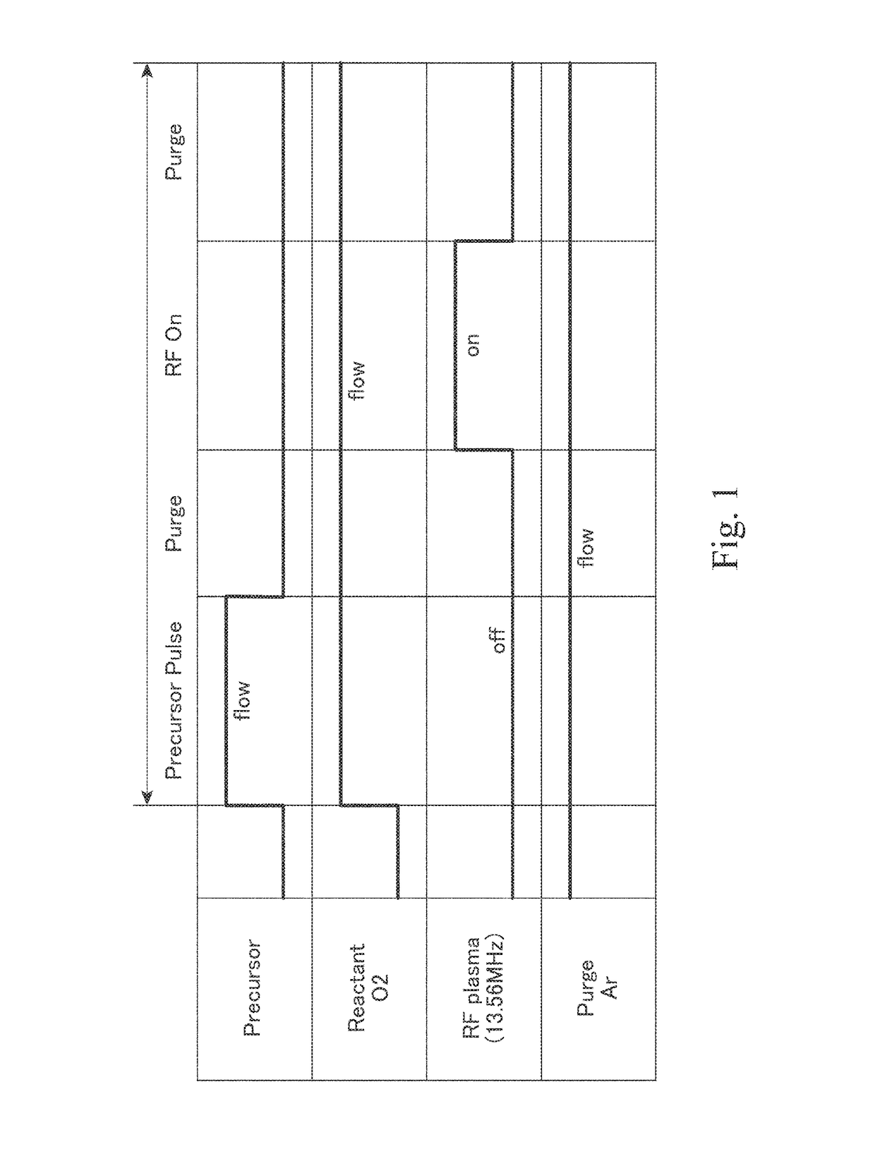
[0048]The film thickness for one cycle is set to 0.1 nm. In depositing a silicon nitride film, Ar was also used throughout the cycle as a purge gas to flow into the reactor and the flow remained at a constant rate. A silicon-containing precursor is supplied with a single pulse, while nitrogen reactant gas or nitrogen and hydrogen reactant gas is introduced to the reactor continuously at a constant rate. After t...
example 2
[0055]Deposition of a Silicon Oxide Film
[0056]A silicon oxide film was deposited on a substrate having recesses or grooves during the deposition session and a Capacitively Coupled Plasma (CCP) device was used as the ALD apparatus. The film deposition conditions were as follows:
[0057]Substrate temperature: 100° C.
[0058]Film deposition pressure: 1.0 Torr
[0059]Silicon-containing precursor: BDEAS
[0060]Silicon-containing precursor pulse: 0.5 second
[0061]Flow rate of oxygen: 1000 sccm
[0062]Flow rate of purge gas (Ar): 1000 sccm
[0063]RF power (13.56 MHz): 100-900 W
[0064]The film thickness for one cycle is set to 0.1 nm. In depositing a silicon oxide film, Ar was used throughout the cycle as a purge gas to flow into the reactor and the flow remained at a constant rate. A silicon-containing precursor is supplied with a single pulse, while oxygen reactant gas is introduced to the reactor continuously at a constant rate. After the silicon-containing precursor pulse stops and the unabsorbed sil...
example 3
[0069]Etching of a silicon oxide or silicon nitride film
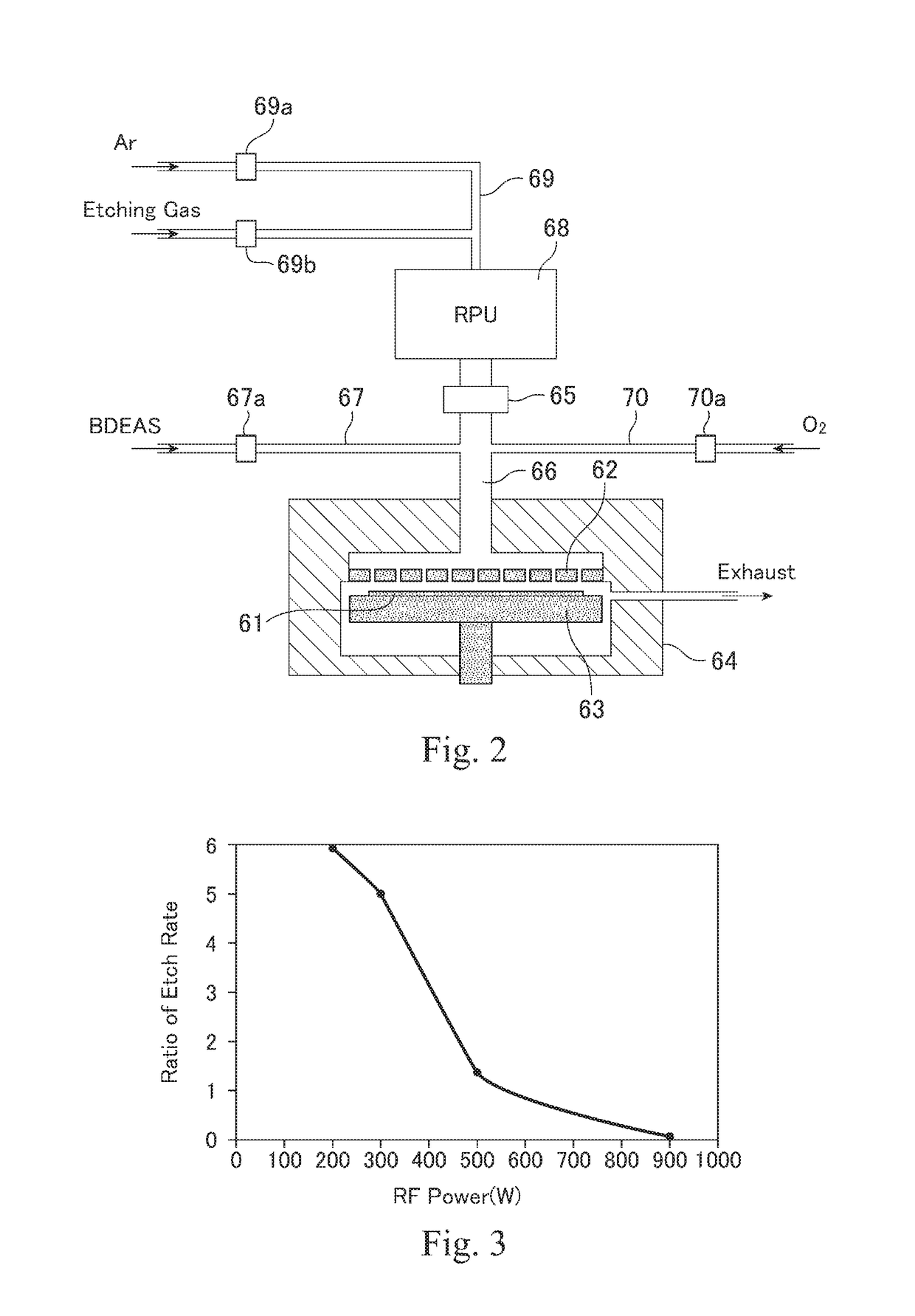
[0070]A silicon oxide film or a silicon nitride film on a substrate having recesses or grooves was then etched by an etching gas, which is activated by a Remote Plasma Unit. The film etching conditions were as follows:
[0071]Substrate temperature: 100° C.
[0072]Film deposition pressure: 1.0-10.0 Torr
[0073]Etching gas: NF3, NF3+NH3 or NF3+O2
[0074]Flow rate of etching gas: 10-200 sccm
[0075]Flow rate of purge gas (Ar): 1-10 slm
[0076]RF power: 1K-5K W
[0077]Etching gas supply time: Continuously supplied during etching session
[0078]Etching rate: 40 nm / min
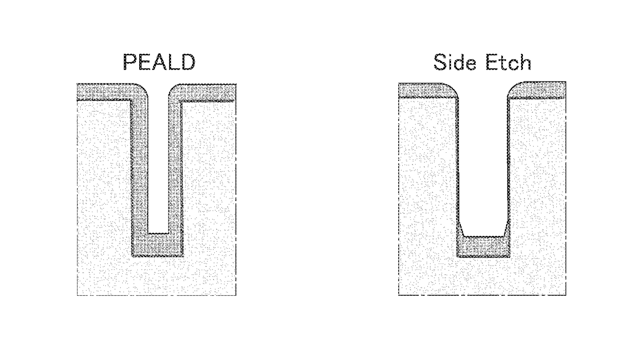
[0079]After the deposition of different film quality by ALD, the thickness of the film deposited on a side wall and top wall of recesses or grooves on a substrate was approximately 10 nm. The etching rate in this example was set at 40 nm / min and the plasma power was set at 1K-5K W. It was found out that due to different film quality between film deposited on the side wall of recesses ...
PUM
 Abstract
Description
Claims
Application Information