Plasma processing apparatus and plasma processing method

a processing apparatus and plasma technology, applied in plasma welding apparatus, solid-state diffusion coating, manufacturing tools, etc., can solve the problems of difficult to clean the inner wall to a sufficient degree, large impurities tend to contaminate into the film, and objects to be contaminated, etc., to achieve the effect of eliminating defects inheren

Inactive Publication Date: 2006-05-25
TOKYO ELECTRON LTD
View PDF18 Cites 226 Cited by
  • Summary
  • Abstract
  • Description
  • Claims
  • Application Information

AI Technical Summary

Benefits of technology

[0010] It is an object of the present invention to provide a plasma processing apparatus and a plasma processing method eliminating the defects inherent in the prior technology.
[0011] Another object of the present invention is to provide a plasma processing apparatus and a plasma processing method effectively preventing the sputtering and the etching of the inner wall of the plasma processing chamber while suppressing the contamination to the object.
[0012] The inventors have conducted a keen study and have discovered that the above object can be achieved very effectively if an oxide film is formed on the inner wall of the plasma processing chamber (and / or on the part constituting the inner wall) by utilizing the plasma processing itself instead of separately executing the Alumite treatment or the ceramic coating that has heretofore been effected.
[0016] In the invention having the above-mentioned constitution, the contaminating metals themselves present in the inner-wall of the plasma processing chamber are not only removed by sputtering based on the plasma processing for cleaning but also an oxide film is formed maintaining a predetermined thickness (e.g., about 10 nm to 100 nm) on the surfaces of the inner wall of the plasma processing chamber making it possible to effectively suppress the occurrence of contamination in the subsequent treatment with the plasma.

Problems solved by technology

In this case, ions contained in the plasma generated in the plasma processing chamber impinge on the inner, wall of the plasma processing chamber, whereby the metal constituting the inner wall is sputtered and / or etched often causing the object to be contaminated.
In the step of treating with Alumite or forming the ceramic coating, however, a considerable impurity tends to contaminated into the film.
Once such impurity is contaminated, it becomes very difficult to clean the inner wall to a sufficient degree after coated with the film despite the inner wall of the plasma processing chamber is subjected to cleaning is (by using, for example, hydrofluoric acid).
When the object is treated with the plasma in the plasma processing chamber that has not been cleaned to a sufficient degree, the impurity is physically discharged by sputtering from the inner wall of the plasma processing chamber due to the irradiation with irons produced by the plasma, and deposit on the object giving rise to the occurrence of various problems such as the so-called metal contamination.
The metal contamination tends to become more serious particularly in recent years with an increase in the degree of integration of circuits in the semiconductor devices.

Method used


Image

  • Plasma processing apparatus and plasma processing method
  • Plasma processing apparatus and plasma processing method
  • Plasma processing apparatus and plasma processing method

Examples


example 1

(Cleaning the Wafers)

[0068] In the present invention, the sampling wafer, the monitoring wafer or the wafer to be put to the ordinary plasma processing, is, usually, subjected to cleaning in a manner as described below.

(1) Substrate.

[0069] The substrate was a P-type silicon substrate measuring 20 cm (8 inches) having a resistivity of 1 Ω-cm and a plane orientation (100).

(2) Cleaning prior to oxidizing the gate.

[0070] A native oxide film and contaminating elements (metals, organic matters, particles) were removed by the RCA cleaning,of a combination of APM (a mixed solution of ammonia:hydrogen peroxide:pure water=1:2:10, 60° C.), HFM (a mixed solution of hydrochloric acid:hydrogen peroxide solution:pure water=1:1:10, 60° C.) and DHF (a mixed solution of hydrofluoric acid pure water=1:100, 23° C.). The RCA cleaning consisted of APM, 10 minutes→rinse with pure water, 10 minutes→DHF, 3 minutes→rinse with pure water, 10 minutes→HPM, 10 minutes→rinse with pure water, 10 minutes→fi...

example 2

(Coating the Treatment Chamber with an Oxide Film by using the Pre-Treating Plasma)

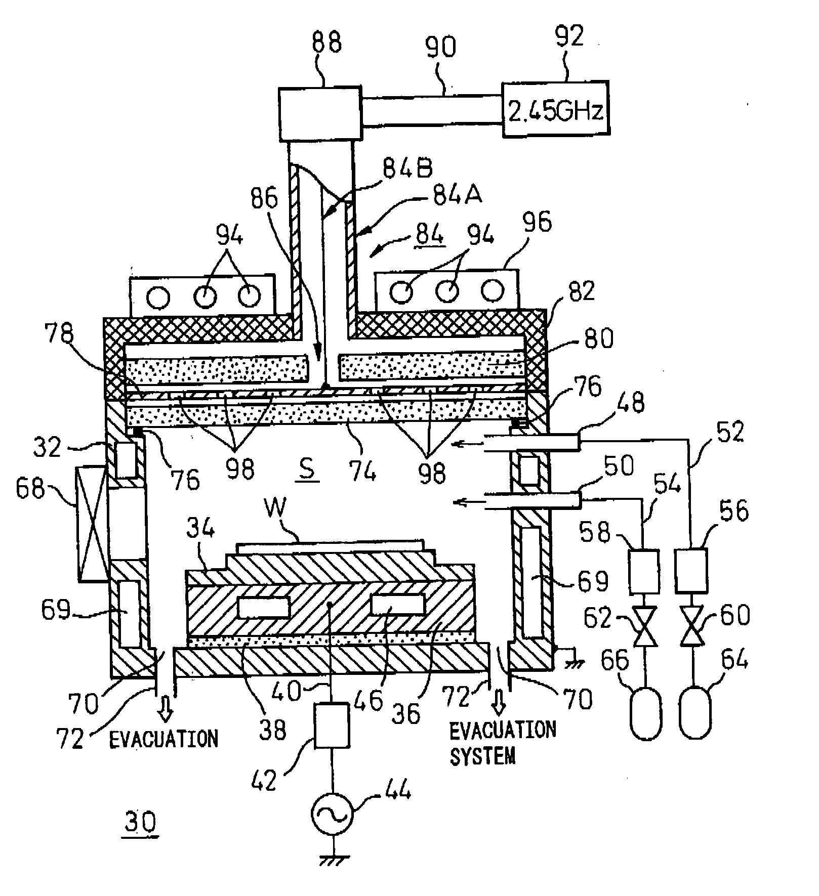
[0071] Referring to FIG. 1, the interior of the plasma processing chamber was coated with an oxide film by using a silicon wafer (sample wafer) W subjected to cleaning as in Example 1.

example 3

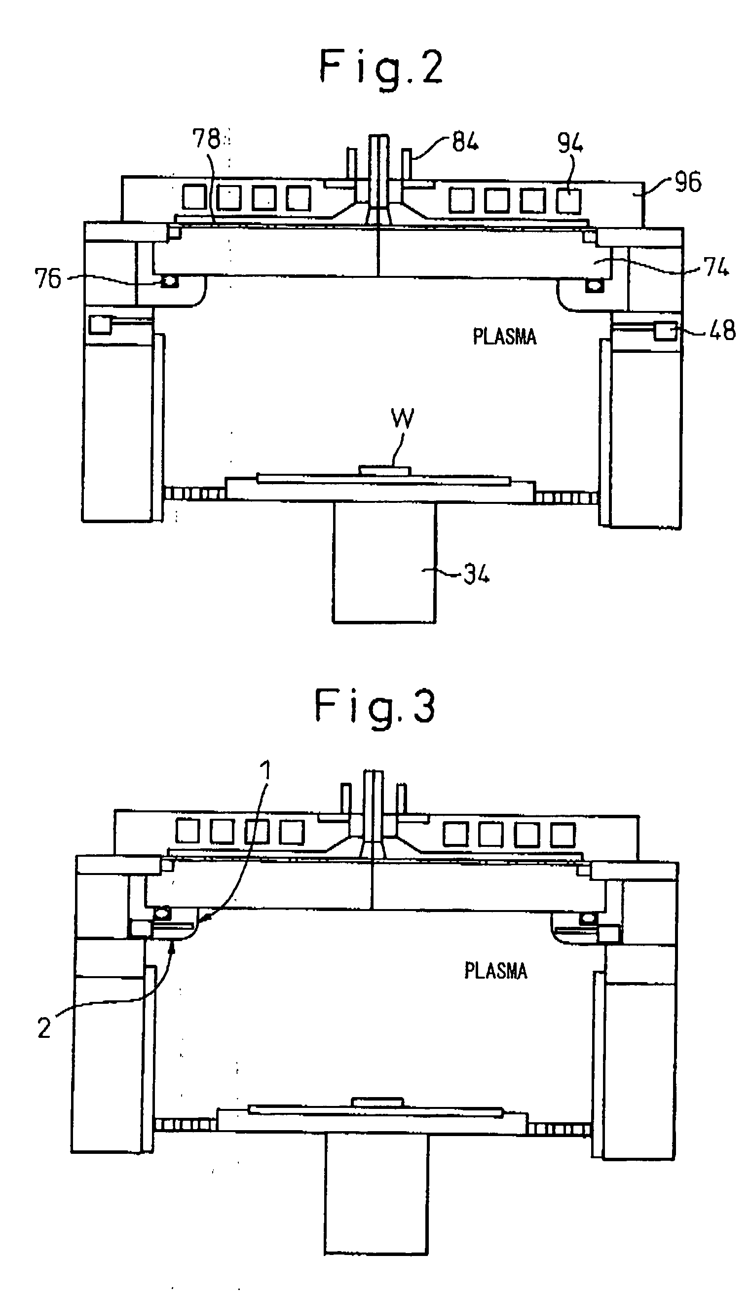
(Oxidation with Plasma by using an Aluminum Member)

[0072] By using a plasma processing apparatus shown in FIG. 2, the oxidizing treatment was conducted under the following plasma processing conditions to observe the oxidized state of the aluminum member forming the inner wall of the plasma processing chamber. The observed places were as shown in a schematic sectional view of FIG. 3.

Plasma Processing Conditions

[0073] Ar / O2=1000 / 10 (sccm)

[0074] Pressure: 6.7 Pa

[0075] Plasma output: 2500 W

[0076] Temperature: 400° C.

[0077] Time; 60 minutes

[0078] The results obtained by the above experiment are shown in Table 1, in the scanning electron microscopic (SEM) photographs of FIGS. 4(a) to 4(d) and in the Auger analytical results of FIG. 5.

Table 1

[0079] Thickness of aluminum oxide film

PlaceFilm ThicknessVertical portion ①-1 9.3 nmVertical portion ①-210.7 nmHorizontal portion ②-122.5 nmHorizontal portion ②-217.2 nm

[0080] The vertical portion (1) and the horizontal portion (2) in T...


PUM

PropertyMeasurementUnit
thicknessaaaaaaaaaa
thicknessaaaaaaaaaa
thicknessaaaaaaaaaa

Abstract

A plasma processing apparatus comprising at least a plasma processing chamber for plasma-processing an object; object-holding means for disposing the object in the plasma processing chamber; and plasma-generating means for generating a plasma in the plasma processing chamber. The inner wall of the plasma processing chamber is at least partially covered with an oxide film based on a pre-treating plasma. A plasma processing apparatus and a plasma processing method effectively prevent the spluttering and the etching of the inner wall of the plasma processing chamber while suppressing contamination to the object.

Description

TECHNICAL FIELD [0001] The present invention relates to a plasma processing apparatus that can be favorably used for putting an object to be treated (or an object to be processed) to a variety of treatments with plasma for producing electronic devices, and to a plasma processing method. BACKGROUND ART [0002] The plasma processing apparatus of the present invention can be extensively used for the treatment with a plasma, such as producing semiconductors or semiconductor devices and electronic device materials like liquid crystal devices. Here, however, the description deals with the background art for semiconductor devices. [0003] In the step of producing semiconductor devices, in general, a base member (wafer) for a semiconductor device that is to be treated is subjected to various treatments such as oxidizing treatment, CVD (chemical vapor deposition) treatment, etching treatment, sputtering treatment and the like treatments. [0004] So far, a plasma processing apparatus has in many...

Claims


Application Information

Patent Timeline
Patent Type & Authority Applications(United States)
IPC IPC(8): B23K10/00C23C16/44H01J37/32H01L21/205
CPCH01J37/32192C23C16/4404
Inventor NOZAWA, TOSHIHISASASAKI, MASARUINOUE, MASAJI
Owner TOKYO ELECTRON LTD
Why Eureka
Try Eureka