Laminated semiconductor substrate process for producing the same

a technology of laminated semiconductor and substrate, which is applied in the direction of semiconductor devices, solid-state devices, basic electric elements, etc., can solve the problems of affecting the production efficiency of the active layer, the roughness of the top surface of the active layer is quite significant, and the delay signal over a wired line has become a critical problem, etc., to achieve the effect of reducing surface roughness, reducing cost and simplifying the process

Inactive Publication Date: 2006-06-08
SUMCO CORP +1
View PDF1 Cites 232 Cited by
  • Summary
  • Abstract
  • Description
  • Claims
  • Application Information

AI Technical Summary

Benefits of technology

[0065] According to the bonded substrate in accordance with the first invention and the manufacturing method of a bonded substrate in accordance with the second invention, after the active layer having been formed by cleaving off a portion of the active layer wafer, the surface of the active layer is etched only by the thickness of 1 nm to 1 μm with the solution having the etching effect. AS a result, the final active layer thickness will be no greater than 20 nm. The final active layer means an active layer at the stage where the etching, polishing and the like have been previously done and then the final cleaning process has been finished. Owing to these processes, the film thickness of the active layer after the cleavage is made uniform over the entire surface area thereof and also these can advantageously simplify the process for achieving the lower surface roughness and accordingly reduce the cost therefor. Further advantageously, due to the fact that this etching is the wet etching, such as dipping in the etchant, the batch processing for handling a plurality of wafers all at once may be employable, thereby allowing the process time to be shorter and thus the throughput to be increased. Furthermore, differently from the conventionally practiced hydrogen annealing, oxide film removal and dry etching, the process of the present invention is carried out without using the heat treatment, and so there could be almost no fear that any metal contamination is induced in the active layer.
[0066] Especially, according to the manufacturing method of a bonded substrate in accordance with the eighth to the thirteenth inventions, after the etching process, the thickness of the active layer is measured, and based on the measured thickness, an amount of subsequent etching can be determined within the range of 1 nm to 1 μm so as to repeat the etching process. This advantageously allows the uniformity in thickness to be achieved over the entire surface area of the active layer in a stable manner.
[0067] According to the manufacturing method of a bonded substrate in accordance with the fourteenth to the sixteenth inventions, since at least one of the steps of: (1) chemical mechanical polishing; (2) hydrogen annealing; and (3) oxide film removal, may be applied to the surface of the active layer of the bonded substrate before and / or after the etching process, the uniformity in film thickness of the active layer after the cleavage can be enhanced and the roughness of the surface of the active layer can be reduced.

Problems solved by technology

On the other hand, in the circumstances where the demand for the higher integration and multi-functionality of an LSI to be constructed on the silicon substrate is getting stricter, a delayed signal over a wired line has become a critical problem.
In the viewpoint of micro surface, however, roughness of the top surface of the active layer is quite significant.
The damage layer in the active layer surface would be an obstacle in forming the device and accordingly needs to be removed.
However, there have been the following defects in association with the manufacturing method of the SOI according to the above-described prior art bonding methods.
Among those, there has been a fear that the film thickness distribution in the active layer could be worse upon applying the chemical mechanical polishing to the surface of the active layer by using a polishing apparatus.
Since this tendency could be more critical as the thickness to be removed in the CMP increases, there has been a limitation in achieving the preparation of the film thickness of the active layer only by the CMP.
Especially, when the active layer thickness is made as thin as 200 nm or lower, there has been observed another problem that the peel-off of the active layer occurs during the CMP process due to a micro void existing in a bonding interface.
This has made the process more complicated and led to higher cost.
In addition, when such a large-sized wafer that has a diameter of 300 mm is subject to the hydrogen annealing, a single wafer processing method has been commonly practiced and this has led to lower throughput.
According to the instant oxide film removal method, the entire procedure has been made complicated as described above and so a long processing time has been required.
Further disadvantageously, it has likely been to lead to cost increase.
Furthermore, since the heat treatment is involved, there has been a possibility that metal contamination could be induced in the active layer.

Method used


Image

  • Laminated semiconductor substrate process for producing the same
  • Laminated semiconductor substrate process for producing the same
  • Laminated semiconductor substrate process for producing the same

Examples


first embodiment

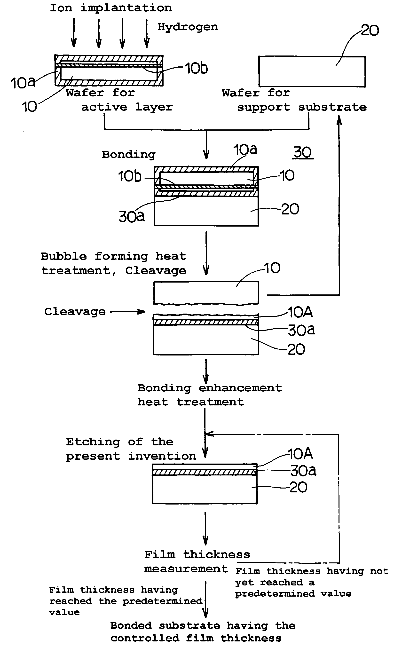
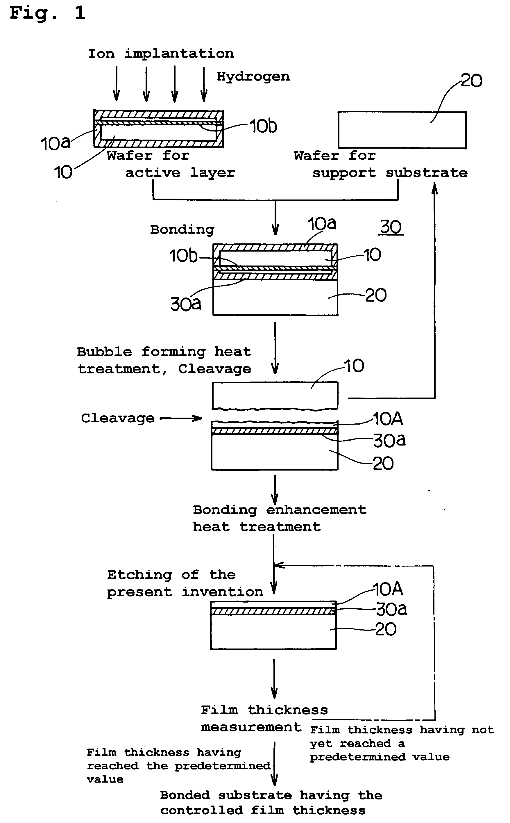
[0074]FIG. 1 is a flow chart showing a manufacturing method of a bonded substrate (SOI substrate) according to the present invention.

[0075] As shown in FIG. 1, firstly a wafer for active layer (silicon wafer) 10 is prepared by applying to a single-crystal silicon ingot that has been pulled up by the CZ method, each of the processes including slicing, beveling, lapping, etching and polishing so as to form it into a wafer having a thickness of 725 μm and a diameter of 200 mm (8 inches) with one-side or both-sides thereof mirror finished. On the other hand, a wafer for support substrate (silicon wafer) 20 is prepared by using the same manufacturing method as that used for the wafer for active layer 10 so as to be formed into a wafer having the same thickness and the same diameter as the wafer for active layer and a mirror finished surface. The active layer wafer 10 from those two is introduced into a thermal oxidation furnace, where it is treated with the thermal oxidation at 900° C. w...

second embodiment

[0087] the present invention will now be described with reference to FIG. 2.

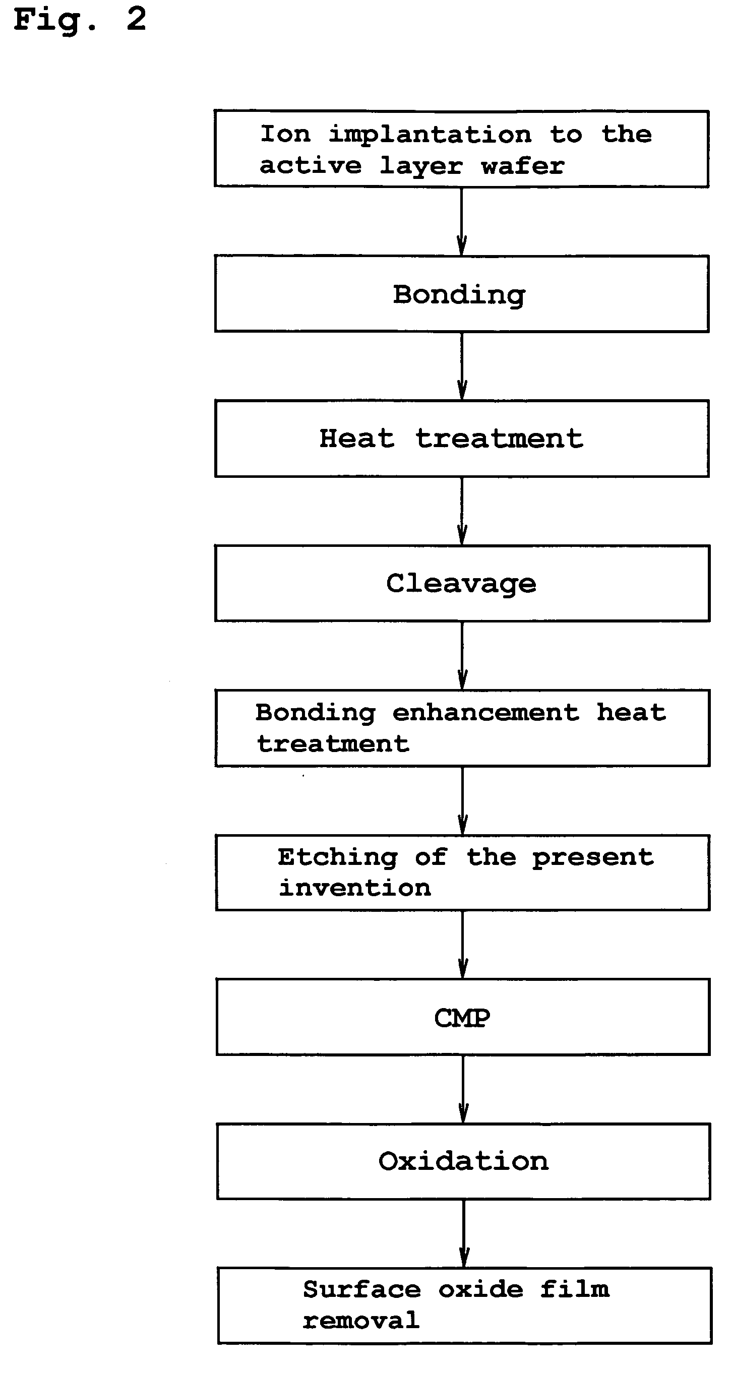
[0088]FIG. 2 is a flow chart showing a manufacturing method of a bonded substrate (SOI substrate) according to the second embodiment.

[0089] In the second embodiment, following to the same procedure as in the first embodiment, the process begins with the hydrogen ion implantation to the active layer wafer, then goes through the bonding of the active layer wafer with the support substrate wafer, the cleavage heat treatment for the bubble formation in the bonded wafer, the cleaving of the active layer wafer at its portion of the ion-implanted region, and the bonding heat treatment for enhancing the bonding strength of the bonded wafer, and finally provides the etching of the surface of the active layer by a predetermined amount by using the SC-1 cleaning fluid. This embodiment is specific in that subsequently the CMP process, the oxidation and the oxide film removal are sequentially applied to the surface of t...

third embodiment

[0098] the present invention will now be described.

[0099]FIG. 3 is a flow chart showing a manufacturing method of a bonded substrate (SOI substrate) according to the third embodiment of the present invention.

[0100] In this embodiment, following to the same procedure as in the second embodiment, the process begins with the hydrogen ion implantation into the active layer wafer, then goes through the bonding of the active layer wafer with the support substrate wafer, the heat treatment for the bubble formation in the bonded wafer, the cleaving of the active layer wafer at its portion of the ion-implanted region, and the bonding heat treatment for enhancing the bonding strength of the bonded wafer, and finally provides the etching of the surface of the active layer by using the SC-1 cleaning fluid. This embodiment is specific in that subsequently the oxidation and the oxide film removal are sequentially applied to the surface of the active layer.

[0101] In this case, the surface roughn...


PUM

PropertyMeasurementUnit
thicknessaaaaaaaaaa
thicknessaaaaaaaaaa
pHaaaaaaaaaa

Abstract

The present invention provides a bonded substrate fabricated to have its final active layer thickness of 200 nm or lower by performing the etching by only 1 nm to 1 μm with a solution having an etching effect on a surface of an active layer of a bonded substrate which has been prepared by bonding two substrates after one of them having been ion-implanted and then cleaving off a portion thereof by heat treatment. SC-1 solution is used for performing the etching. A polishing, a hydrogen annealing and a sacrificial oxidation may be respectively applied to the active layer before and/or after the etching. The film thickness of this active layer can be made uniform over the entire surface area and the surface roughness of the active layer can be reduced as well.

Description

FIELD OF THE INVENTION [0001] The present invention relates to a bonded semiconductor substrate and a manufacturing method thereof, and more particularly to such a bonded semiconductor substrate and a manufacturing method thereof that comprises an active layer formed by cleaving and separating a portion of an active layer substrate, specifically the semiconductor substrate having an uniform thickness of the active layer across an entire surface thereof without inducing any peel-off of the active layer, even if the active layer of thin film has the thickness as thin as 0.2 μm or lower. DESCRIPTION OF THE PRIOR ART [0002] The bonded semiconductor substrate has been broadly studied, especially in the field of semiconductors, from the viewpoint of its feature created by bonding together a support substrate and an active layer substrate having a different property from the support substrate so as to allow the finished bonded semiconductor substrate to have a specific property that is dif...

Claims


Application Information

Patent Timeline
Patent Type & Authority Applications(United States)
IPC IPC(8): H01L21/30H01L23/06H01L27/12H01L21/02H01L21/306H01L21/762
CPCH01L21/30608H01L21/76254H01L21/20H01L27/12
Inventor KAMIYAMA, EIJIKATOH, TAKEOPARK, JEA GUN
Owner SUMCO CORP
Why Eureka
Try Eureka