Method for producing a gallium nitride epitaxial layer

a gallium nitride and epitaxial layer technology, applied in the direction of crystal growth process, crystal growth process, polycrystalline material growth, etc., can solve the problems of preventing the sapphire substrate from being removed, slowed down the development of diode lasers, and not being able to solve this problem, so as to achieve better gan crystal quality

Inactive Publication Date: 2001-12-04
SAINT GOBAIN CRISTAUX & DETECTEURS
View PDF5 Cites 230 Cited by
  • Summary
  • Abstract
  • Description
  • Claims
  • Application Information

AI Technical Summary

Benefits of technology

1010] directions on a dielectric surface, and therefore without being in epitaxial relationship with the sapphire substrate, results in much better GaN crystal quality than the usual processes. After said features have been obtained, the growth ma

Problems solved by technology

However the crystal lattice parameter mismatch between sapphire and GaN is such that the build-up of stresses in the layers results in cracks and prevents the sapphire substrate from being removed.
All the experimental innovations (treatment of the surface of the sapphire at the start of growth with GaCl, deposition of a ZnO interlayer) have not ma

Method used


Image

  • Method for producing a gallium nitride epitaxial layer

Examples


example 2

Deposition in the Gaseous Phase of a Layer of Gallium Nitride To Which Magnesium Has Been Added

The experiment of Example 1 is repeated apart from the fact that 2.8 .mu.mol / min. of (MeCp) .sub.2 Mg is introduced in the vapor phase. The conditions used are: growth time 30 min., growth temperature 1080.degree. C., TMGa 16 .mu.mol / min. and N.sub.2, H.sub.2 and NH.sub.3 2 sl / min. for each of them.

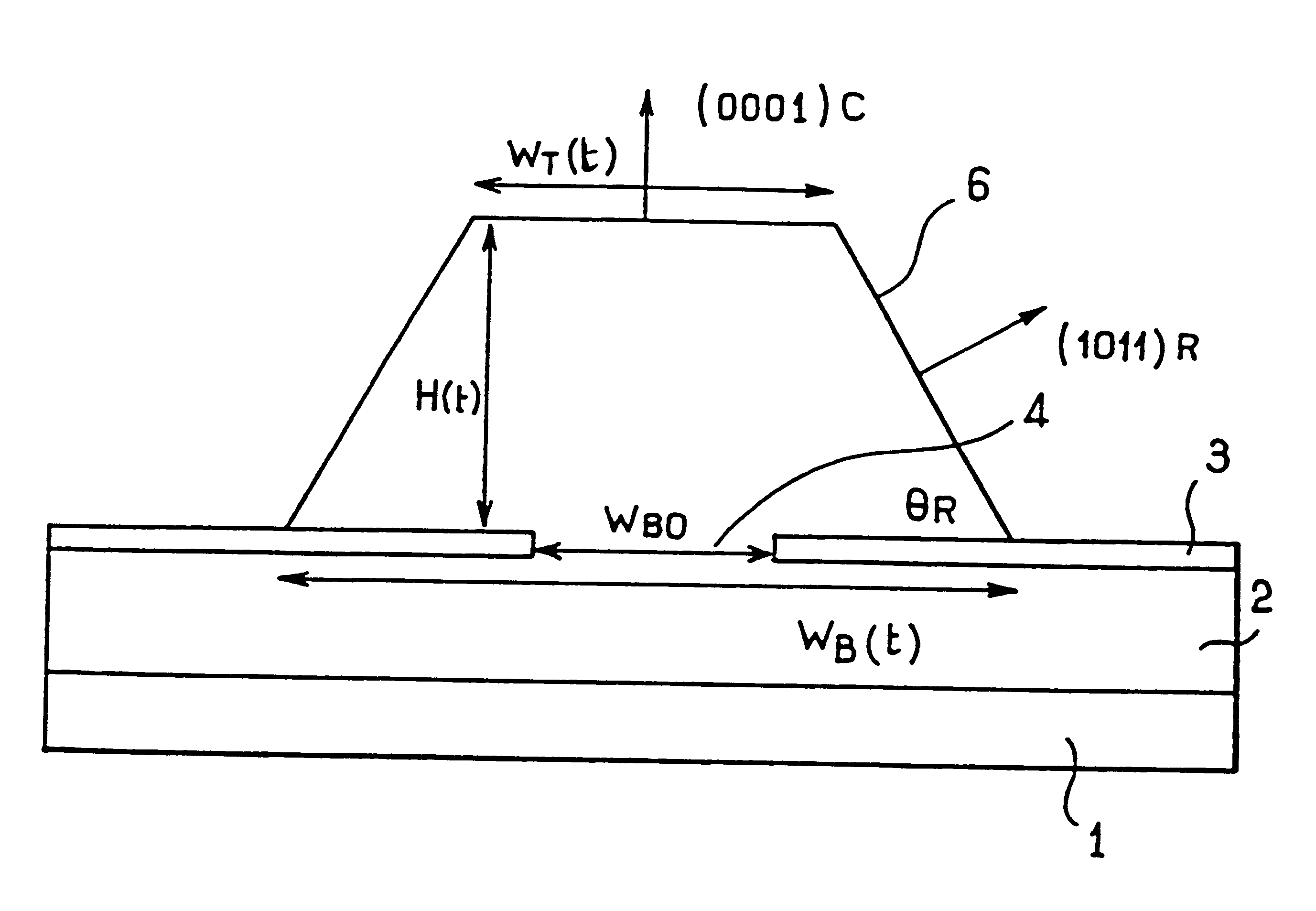
FIG. 6 shows that the presence of magnesium increases the V.sub.R / V.sub.C ratio well above the cos (.theta..sub.R) threshold and consequently the (0001) upper facet broadens. The selectivity of the growth is not affected by the presence of (MeCp).sub.2 Mg, but the growth anisotropy is advantageously modified.

example 3

Influence of the Mg / Ga Molar Ratio

FIG. 5 shows the variation in the growth rates normalized to the TMGA molar flux in the [0001] and [1011] directions as a function of the Mg / Ga molar ratio in the vapor phase.

In practice, it was chosen to keep a constant flux of (MeCp).sub.2 Mg and to vary the amount of TMGA. This makes it possible to ensure that the available Mg concentration on the surface of the growth islands is identical for all the specimens.

Because the growth is controlled linearly by the amount of gallium supplied, the growth rates are normalized in order to compare them.

V.sup.N.sub.C rapidly decreases from 0.8 to 0.1 .mu.m / h / .mu.mol, while V.sup.N.sub.R increases from 0.16 to 0.4 .mu.m / h / .mu.mol when the Mg / Ga molar ratio varies from 0 to 0.17. The dotted line is the curve of the V.sub.R / V.sub.C ratio obtained by extrapolation. The y-axis on the right is V.sub.R / V.sub.C .

This curve shows that the incorporation of Mg allows the pyramidal structure to be easily controlled b...

example 4

Two-step Deposition of a Gallium Nitride Layer

Firstly, the process according to the invention is carried out using epitaxial regrowth under operating conditions comparable to those of Example 1.

An SiN mask is deposited on a GaN layer deposited beforehand in an epitaxial manner in a suitable reactor on a crystallization substrate such as sapphire. Linear apertures 5 .mu.m in width and spaced apart by 5 .mu.m are then made in the mask in order to expose the regions of the subjacent layer. The linear apertures are advantageously oriented in the GaN [1010] direction, although the variant of the process described in this example can be optionally carried out for other orientations of the linear apertures, especially in the GaN [1120] direction.

The epitaxial regrowth is carried out on the exposed regions with unintentionally doped GaN under operating conditions such that the growth rate in the [0001] direction of the GaN features sufficiently exceeds the growth rate in the direction norma...


PUM


Abstract

The invention concerns a method for producing a gallium nitride (GaN) epitaxial layer characterised in that it consists in depositing on a substrate a dielectric layer acting as a mask and depositing on the masked gallium nitride, by epitaxial deposit, so as to induce the deposit of gallium nitride patterns and the anisotropic lateral growth of said patterns, the lateral growth being pursued until the different patterns coalesce. The deposit of the gallium nitride patterns can be carried out ex-situ by dielectric etching or in-situ by treating the substrate for coating it with a dielectric film whereof the thickness is of the order of one angstrom. The invention also concerns the gallium nitride layers obtained by said method.

Description

The present invention relates to a process for producing an epitaxial layer of gallium nitride (GaN) as well as to the epitaxial layers of gallium nitride (GaN) which can be obtained by said process. Such a process makes it possible to obtain gallium nitride layers of excellent quality.It also relates to the short-wavelength optical devices or the high-power high-frequency electronic devices provided with such an epitaxial gallium nitride layer.It relates in particular to optoelectronic components formed on such gallium nitride layers.Processes are known for obtaining relatively thick GaN layers, for example from 100 to 200 micrometers. The method commonly used is chloride and hydride vapor phase epitaxy (HVPE). Either sapphire substrates or GaN layers on sapphire 200 micrometers in thickness are used, these layers being fabricated by OrGaNoMetallic Pyrolisis Vapor Phase Epitaxy (OMVPE). However the crystal lattice parameter mismatch between sapphire and GaN is such that the build-u...

Claims


Application Information

Patent Timeline
IPC IPC(8): C30B25/02H01L21/20H01L21/02H01L33/00H01S5/323H01S5/00C30B29/38
CPCC30B25/02C30B29/406H01L21/0237H01L21/0242H01L21/0254H01L21/02573H01L21/02579H01L21/0262H01L21/02639H01L21/02647H01L33/007H01S5/32341
Inventor BEAUMONT, BERNARDGIBART, PIERREGUILLAUME, JEAN-CLAUDENATAF, GILLESVAILLE, MICHELHAFFOUZ, SOUFIEN
Owner SAINT GOBAIN CRISTAUX & DETECTEURS
Why Eureka
Try Eureka