MTJ MRAM with stud patterning

a technology of stud patterning and mtj, which is applied in the direction of magnetic field-controlled resistors, galvano-magnetic devices, semiconductor devices, etc., can solve the problems of widening (i.e. oversized) and increasing the margin of error, and achieves the effect of higher bias

Active Publication Date: 2014-07-08
AVALANCHE TECH
View PDF8 Cites 216 Cited by
  • Summary
  • Abstract
  • Description
  • Claims
  • Application Information

AI Technical Summary

Benefits of technology

[0007]Embodiments of the invention use a multilayer etching mask that includes a stud mask for MTJ etching to form a sloping sidewall of the barrier layer and to form a bottom electrode that is wider than the rest of the MTJ pillar. The bottom electrode can therefore, be wider (i.e. oversized) than the contact stud and provide increased margin of error for the alignment of the MTJ pillar without increasing the width of the magnetic layers in the MTJ. The first embodiment of the invention described includes a top electrode and a stud mask. In the second and third embodiments the stud mask is a conductive material and also serves as the top electrode.
[0010]In the third embodiment full film layers are deposited as in the first embodiment except that the top electrode layer is omitted. The stud mask is formed as in the first and second embodiments, but the spacer sleeve is formed in a different way by manipulating the electrical bias on the substrate during etching. The first etching phase in this embodiment uses the stud mask (without a sleeve) to etch down through the capping layer and into the upper magnetic layer. A polymer stud spacer sleeve is formed during the etching process by polymer redeposition the pillar sidewall by lowering substrate bias power to promote polymer deposition on the side wall of stud mask and upper magnetic layer. The next etching phase proceeds down through the MTJ layers to the upper surface of the bottom electrode. The polymer sleeve step structure is transferred downward so that the MTJ layers are wider than the stud mask. The next etching phase uses higher bias and proceeds down to the bottom electrode layer. The step structure is again transferred downward so that the lower magnetic layer is wider than the stud mask and the pillar tapers toward the top. The next etching phase proceeds through the bottom electrode to complete the pillar. The tapering step structure is again transferred downward so that the bottom electrode is wider than the MTJ layers and the stud mask. Tapering the sidewall helps to prevent metallic re-deposition that bridges a free layer and a pinned layer. A capping layer is deposited and a bit line interconnection process is performed.

Problems solved by technology

The bottom electrode can therefore, be wider (i.e. oversized) than the contact stud and provide increased margin of error for the alignment of the MTJ pillar without increasing the width of the magnetic layers in the MTJ.

Method used


Image

  • MTJ MRAM with stud patterning
  • MTJ MRAM with stud patterning
  • MTJ MRAM with stud patterning

Examples


first embodiment

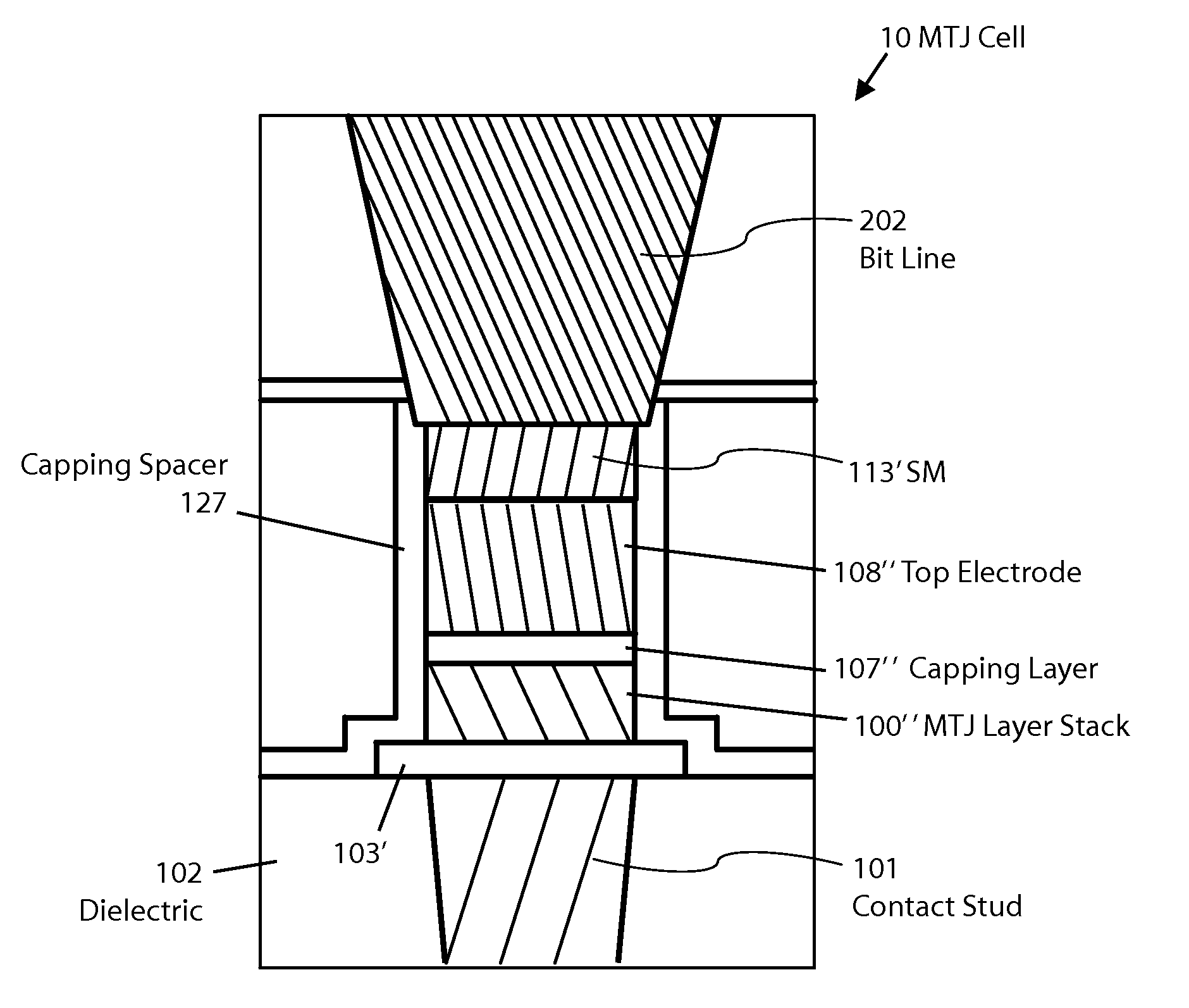
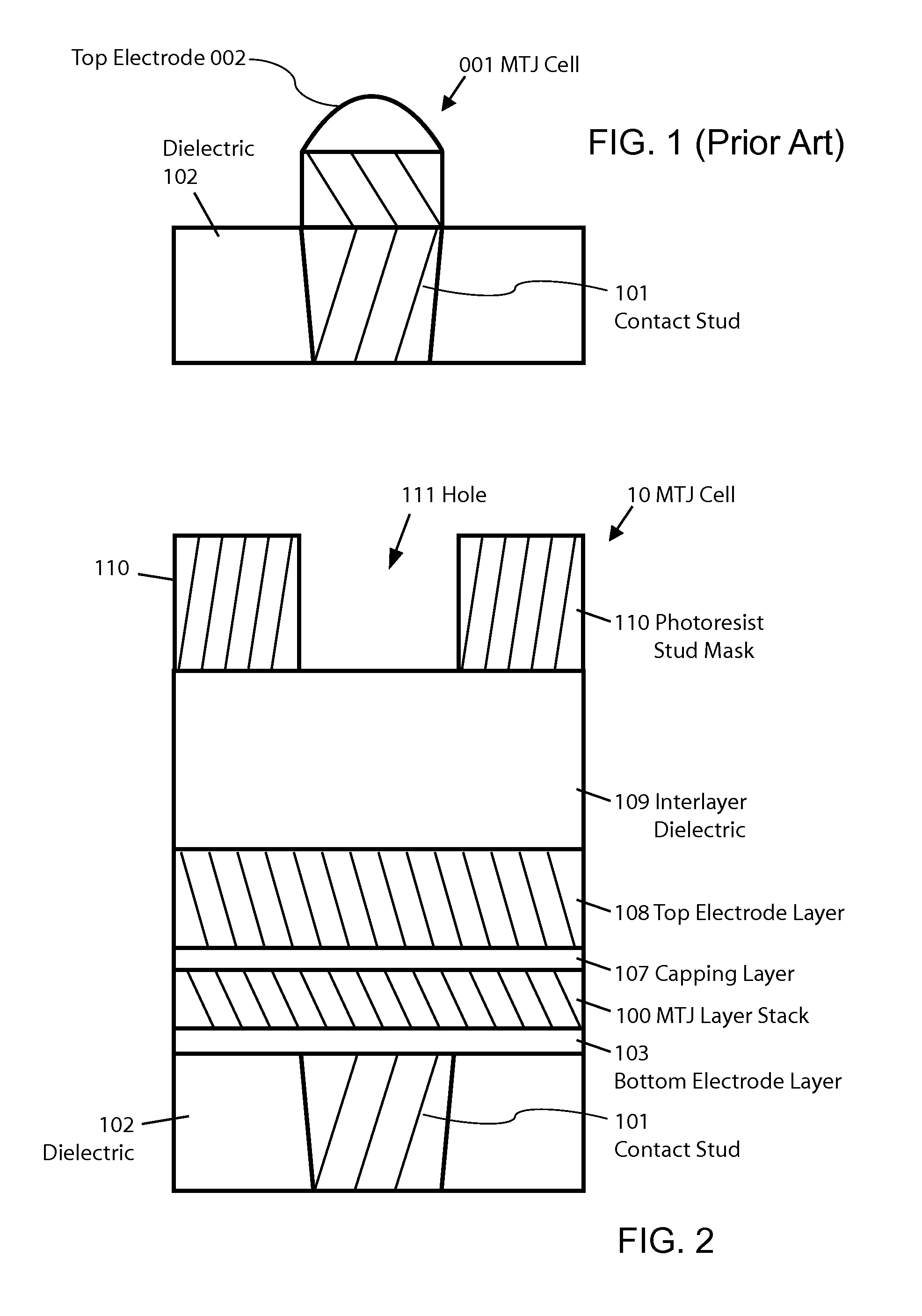
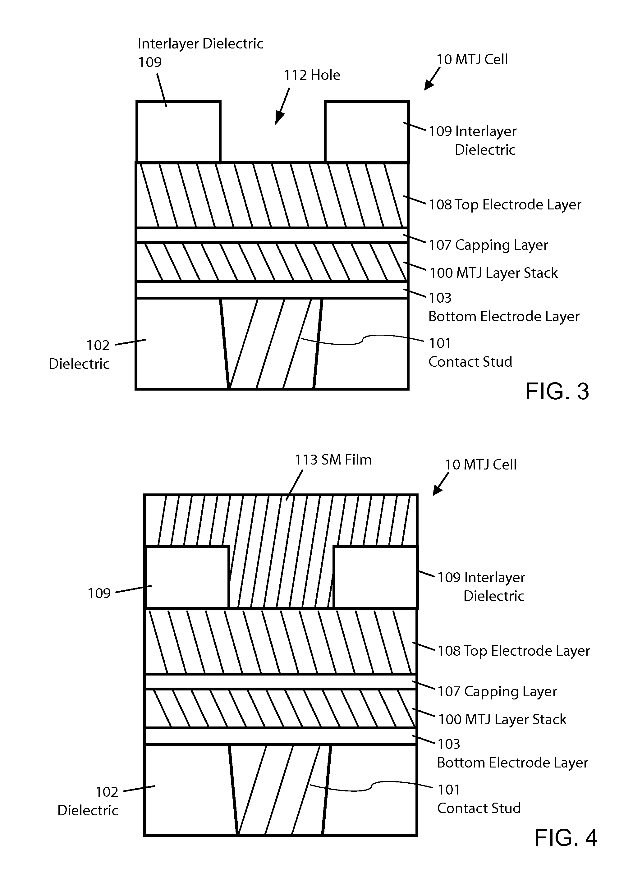
[0042]FIGS. 2 to 6 will be used to describe the stud mask (SM) fabrication process of the first embodiment of the invention. FIG. 2 illustrates a selected stage of the MTJ MRAM fabrication process for MTJ cell 10. FIG. 2 illustrates that the fabrication process has previously patterned landing pad or contact stud 101 which is isolated by interlayer dielectric layer 102 in the conventional way. The plurality of layers for the MRAM cell have been deposited in sequence over the wafer with no patterning. The lowest layer in the cell is the bottom electrode (BE) layer 103, which is followed by the multiple layers in the MTJ layer stack 100 which includes conventional layers (not shown) such as the free and pinned magnetic layers and the barrier layer. Because the magnetic free layer, for example, can be the upper or the lower magnetic according standard MTJ principles, the following description will typically refer only to the upper and lower magnetic layers with the understanding that t...

second embodiment

[0053]FIGS. 16 to 22 illustrate the second embodiment. In this embodiment the stud mask (SM) 213 also works as a top electrode as well in MTJ Cell 12. The SM 213 fabrication process for the second embodiment of the invention is the same as in the first embodiment except that the SM 213 is formed on top of the capping layer 107 and the SM 213 is preferably thicker than SM 113′. The absence of the separate top electrode layer from the second embodiment results in the exposure of the capping layer where the TE was exposed in the first embodiment. Thus, the capping layer will protect MTJ stacks from the ILD etching ambient.

[0054]FIGS. 16 and 17 illustrate the fabrication process of the stud spacer 215. In FIG. 16 the stud mask 213 has been patterned as previously described. The stud spacer layer 215 has been deposited to conform to the underlying topography as shown. The material for the stud spacer layer 215 is same as described in the first embodiment. FIG. 17 shows the result of dire...

third embodiment

[0060]The SM fabrication process for the third embodiment of the invention is processed in the same manner as the second embodiment of the invention with the absence of TE. FIG. 23 illustrates subsequent stage after the SM 213 is fabricated for MTJ Cell 13. The remainder process for the third embodiment is different from the first and the second embodiments of the invention. The stud mask spacer sleeve in this embodiment is formed by polymers created during the etching process. Typically net deposition of materials during an etching process is avoided but this embodiment takes advantage of the phenomenon to achieve a desired result. At first the MTJ etching is performed using standard bias parameters, but when MTJ etching reaches the approximate middle of the upper magnetic layer 100U, the substrate bias is lowered below the standard level to allow a net build up of polymer stud spacer 301 on sidewall of the stud mask and the plateau portion of the upper magnetic layer 100U as shown...


PUM


Abstract

Use of a multilayer etching mask that includes a stud mask and a removable spacer sleeve for MTJ etching to form a bottom electrode that is wider than the rest of the MTJ pillar is described. The first embodiment of the invention described includes a top electrode and a stud mask. In the second and third embodiments the stud mask is a conductive material and also serves as the top electrode. In embodiments after the stud mask is formed a spacer sleeve is formed around it to initially increase the masking width for a phase of etching. The spacer is removed for further etching, to create step structures that are progressively transferred down into the layers forming the MTJ pillar. In one embodiment the spacer sleeve is formed by net polymer deposition during an etching phase.

Description

FIELD OF THE INVENTION[0001]The present invention relates generally to designs and fabrication methods for non-volatile magnetic random access memory (MRAM) and particularly to methods for fabricating resistive memory cells for non-volatile MRAM incorporating a small feature size magnetic tunnel junction (MTJ).BACKGROUND[0002]The memories such as RRAM (Resistive Random Access Memory), PRAM (Phase Change Random Access Memory), and MRAM (Magnetic Random Access Memory) have a resistive device as a memory element. The high speed access and the non-volatility at power off of these devices are promising technologies to replace existing memories.[0003]The resistive memory device consisting of a top electrode, a bottom electrode and the resistive memory element in between is fabricated in a pillar shape using a conventional lithography and dry etching process. The memory element MTJ (Magnetic Tunnel Junction) includes at least a pinned layer, a free layer and barrier layer in between. The c...

Claims


Application Information

Patent Timeline
Patent Type & Authority Patents(United States)
IPC IPC(8): H01L43/12H01L43/00
CPCH01L43/08H01L43/12H01L43/02H10N50/01H10N50/10
Inventor JUNG, DONG HASATOH, KIMIHIROZHANG, JINGZHOU, YUCHENHUAI, YIMING
Owner AVALANCHE TECH
Why Eureka
Try Eureka