Leadless plastic chip carrier with standoff contacts and die attach pad

a leadless, chip carrier technology, applied in the direction of semiconductor devices, semiconductor/solid-state device details, electrical devices, etc., can solve the problems of limiting the packaging density of such prior art devices, and achieve the effects of improving motherboard assembly, reducing solder joint stress, and improving solder assembly

Active Publication Date: 2006-05-23
UTAC HEADQUARTERS PTE LTD
View PDF12 Cites 217 Cited by
  • Summary
  • Abstract
  • Description
  • Claims
  • Application Information

AI Technical Summary

Benefits of technology

[0010]The standoff contact pads and die attach pad of the present invention improve motherboard assembly, allowing for better solder assembly to the motherboard and reduced stresses at the solder joints to the motherboard. This is accomplished while maintaining improved package density, thermal performance and electrical performance over traditional QFP packages. Also, undercut etch portio

Problems solved by technology

The inner leads terminate in outer leads that are bent down to contact a mot

Method used


Image

  • Leadless plastic chip carrier with standoff contacts and die attach pad
  • Leadless plastic chip carrier with standoff contacts and die attach pad
  • Leadless plastic chip carrier with standoff contacts and die attach pad

Examples


Embodiment Construction

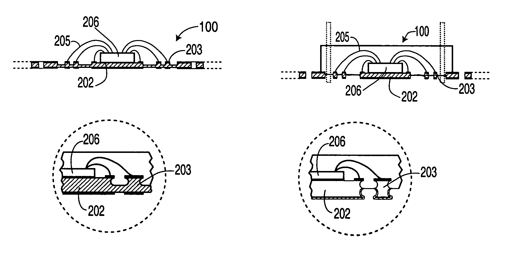
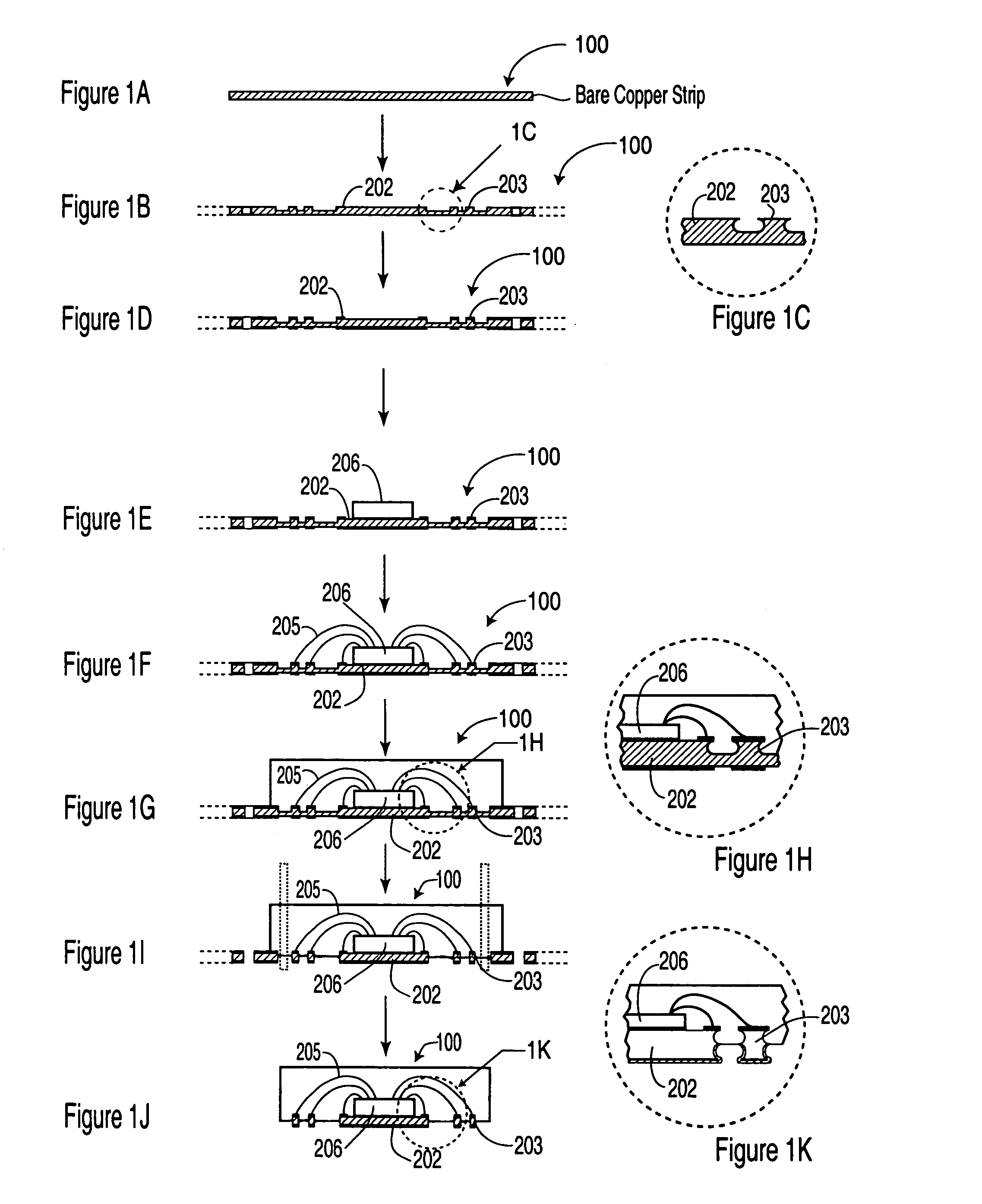
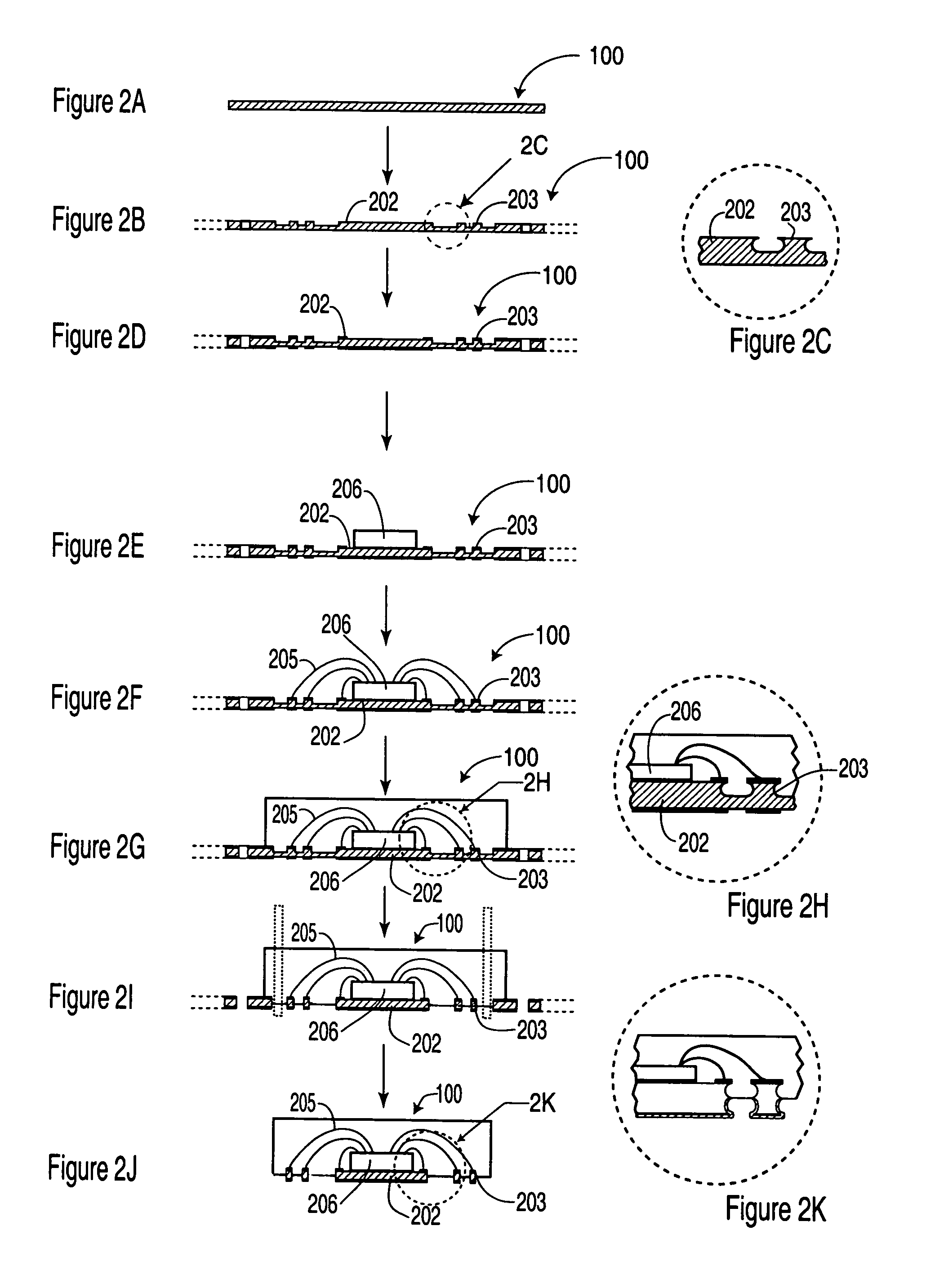
[0017]The present invention relates to an improvement over Applicant's U.S. Pat. No. 6,229,200 for a Saw Singulated Leadless Plastic Chip Carrier (LPCC). Where possible, the same reference numerals have been used in this application to denote identical features described in Applicant's above-noted LPCC patent.

[0018]Reference is first made to FIGS. 1A to 1H to describe the processing steps for manufacturing a LPCC with standoff contacts (contact pads) and die attach pad according to an embodiment of the present invention. FIG. 1A shows an elevation view of a Cu (copper) panel substrate which forms the raw material of the leadframe strip indicated generally by the numeral 100. As discussed in detail in Applicant's U.S. Pat. No. 6,299,200, the leadframe strip 100 is divided into a plurality of sections, each of which incorporates a plurality of leadframe units in an array (e.g. 3×3 array, 5×5 array, etc.). Only one such whole unit is depicted in the elevation view of FIG. 1A, portions ...


PUM


Abstract

A process for fabricating a leadless plastic chip carrier includes selectively etching at least a first surface of a leadframe strip to partially define at least a plurality of contact pads and a die attach pad; selectively plating at least one layer of metal on a second surface of the leadframe strip, on an undersurface of at least the plurality of contact pads and the die attach pad; mounting a semiconductor die on the first surface, on the partially defined die attach pad; wire bonding the semiconductor die to ones of the contact pads; encapsulating the wire bonds and the semiconductor die in a molding material such that the molding material covers a first portion of the die attach pad and first portions of the contact pads; selectively etching a second surface of the leadframe strip to define a second portion of the contact pads and a second portion of the die attach pad by etching the second surface with the at least one layer of metal resisting etching; and singulating the leadless plastic chip carrier from the leadframe strip.

Description

FIELD OF THE INVENTION[0001]The present invention relates in general to integrated circuit packaging and more particularly to an improved leadless plastic chip carrier including standoff contacts.BACKGROUND OF THE INVENTION[0002]According to well known prior art IC (integrated circuit) packaging methodologies, semiconductor dice are singulated and mounted using epoxy or other conventional means onto respective die pads (attach paddles) of a leadframe strip. Traditional QFP (Quad Flat Pack) packages incorporate inner leads which function as lands for wire bonding the semiconductor die bond pads. These inner leads typically require mold locking features to ensure proper positioning of the leadframe strip during subsequent molding to encapsulate the package. The inner leads terminate in outer leads that are bent down to contact a mother board, thereby limiting the packaging density of such prior art devices.[0003]In order to overcome these and other disadvantages of the prior art, the ...

Claims


Application Information

Patent Timeline
IPC IPC(8): H01L21/50
CPCH01L21/4832H01L23/49582H01L24/85H01L23/3107H01L2924/15747H01L2924/014H01L2924/01033H01L2924/00014H01L2224/32245H01L24/48H01L2924/14H01L2924/01082H01L2924/01079H01L2924/01078H01L2924/0105H01L2924/01047H01L2924/01046H01L2924/01029H01L2924/01028H01L24/45H01L2221/68377H01L2224/45144H01L2224/48091H01L2224/48247H01L2224/48257H01L2224/73265H01L2224/85001H01L2224/85464H01L2224/78H01L2924/00H01L2224/48664H01L2924/181H01L2924/00012
Inventor FAN, CHUN HOLAU, WING HIMKWAN, KENNETHWONG, JANET
Owner UTAC HEADQUARTERS PTE LTD
Why Eureka
Try Eureka