Latching micro magnetic relay packages and methods of packaging

a micro magnetic relay and package technology, applied in the field of latching micro magnetic relays, can solve the problems of serious limitations in the process steps performed after the application of the photoresist layer, serious affecting the magnets and other components, and high temperatures for some of the later

Inactive Publication Date: 2006-12-19
SCHNEIDER ELECTRIC IND SAS
View PDF12 Cites 14 Cited by
  • Summary
  • Abstract
  • Description
  • Claims
  • Application Information

AI Technical Summary

Problems solved by technology

One problem with this prior art method is that any process steps performed subsequent to the application of the photoresist layer are seriously limited because of potential damage to the photoresist material and, thus, potential faults or weaknesses in the final product.
Also, in most prior art packaging techniques relatively high temperatures are required for some of the later steps.
These high temperatures can seriously affect magnets and some of the other components enclosed in the packages.
Further, the materials that could be used as the supporting substrate for the MEMS devices is seriously limited by the fabrication and packaging techniques.

Method used


Image

  • Latching micro magnetic relay packages and methods of packaging
  • Latching micro magnetic relay packages and methods of packaging
  • Latching micro magnetic relay packages and methods of packaging

Examples


Embodiment Construction

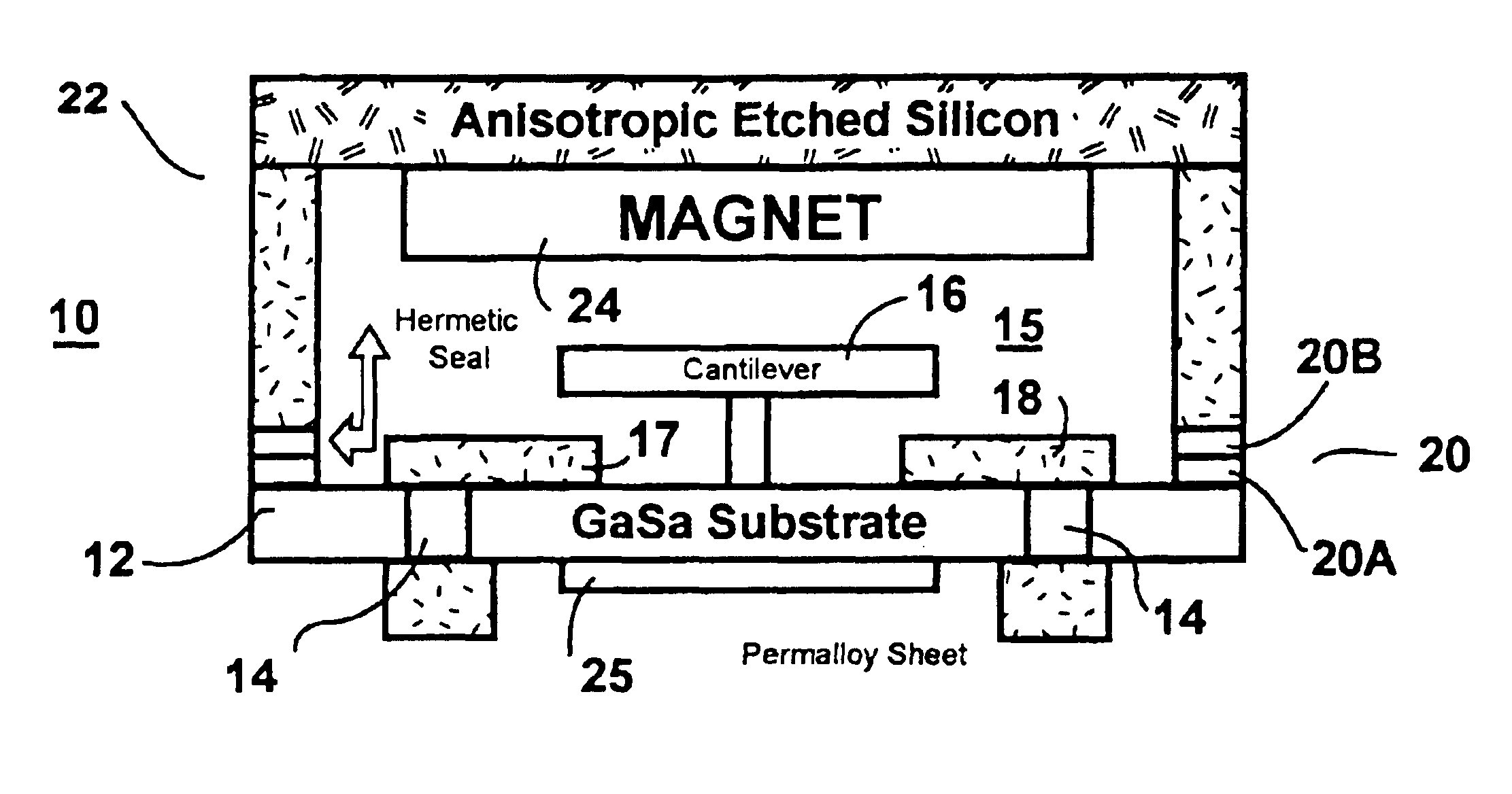
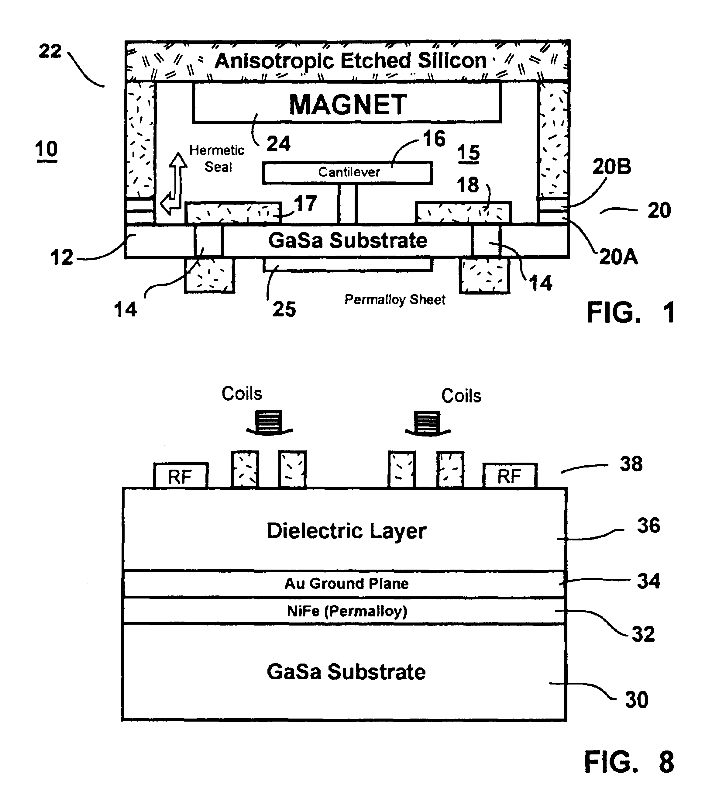
[0024]Turning now to FIG. 1, a wafer scale package 10 is illustrated for a latching micro magnetic relay or other MEMS structures incorporating a magnet or other heat sensitive components. As will be described in more detail below, one major advantage of package 10 is that it can be assembled using solder preforms and low temperature assembly. Low temperature assembly is desirable because the magnet incorporated in the MEMS structure can easily be damaged by too much heat.

[0025]As will become apparent from the discussion below, package 10 can be fabricated in wafer format and does not require the assembly of the MEMS devices individually into individual packages. As described in conjunction with the above structure, a plurality of MEMS devices are generally formed simultaneously on a single wafer. If the wafer must be separated into individual MEMS devices and each individual device packaged separately, the labor cost becomes very high.

[0026]In this specific embodiment, a GaAs subst...


PUM

PropertyMeasurementUnit
conductiveaaaaaaaaaa
magneticaaaaaaaaaa
adhesionaaaaaaaaaa

Abstract

A method of forming a hermetically sealed MEMS package includes a step of providing a supporting GaAs substrate with at least one contact for the MEMS device on the surface of the supporting substrate and forming a cantilever on the surface of the supporting substrate positioned to come into electrical engagement with the contact in one orientation. A metal seal ring is fixed to the surface of the supporting substrate circumferentially around the contact and the cantilever. A cavity is etched in a silicon chip to form a cap member. A metal seal ring is fixed to the cap member around the cavity. The package is hermetically sealed by reflowing a solder alloy, positioned between the two seal rings, in an inert environment without the use of flux.

Description

CROSS-REFERENCE TO RELATED APPLICATION[0001]This application is a division, of application Ser. No. 10 / 126,291, filed Apr. 19, 2002, now U.S. Pat. No. 6,778,046, which claims the benefit of U.S. Provisional Application Ser. No. 60 / 322,841, entitled MICRO MAGNETIC SWITCH FABRICATION AND APPARATUS, filed 17 Sep. 2001.FIELD OF THE INVENTION[0002]This invention relates to latching micro magnetic relays.[0003]More particularly, the present invention relates to methods of packaging latching micro magnetic relays and the various packages.BACKGROUND OF THE INVENTION[0004]Recently, novel latching micro magnetic relays were discovered. The novel latching micro magnetic relay is based on preferential magnetization of a soft magnetic cantilever in a permanent external magnetic field. Switching between two magnetic states is accomplished by momentarily changing the direction of the cantilever's magnetization by passing a short current pulse through a planar coil situated adjacent the cantilever....

Claims


Application Information

Patent Timeline
Patent Type & Authority Patents(United States)
IPC IPC(8): H01H51/22B23K31/02B23K101/40B81B7/00H01H1/00H01H36/00H01H49/00H01H50/00H01H51/24H01L23/10
CPCB81B7/0077H01H1/0036H01H36/0006H01H50/005H01L23/10H01L24/97H01L2924/1461H01L2924/10253H01L2924/01024H01H2036/0093H01H2050/007H01L2924/01013H01L2924/01033H01L2924/01074H01L2924/01078H01L2924/01079H01L2924/09701H01L2924/10329H01L2924/30105H01L2924/01006H01L2924/00H01L2924/0002H01L2924/12042
Inventor STAFFORD, JOHNTAM, GORDONSHEN, JUN
Owner SCHNEIDER ELECTRIC IND SAS
Why Eureka
Try Eureka