Process to improve programming of memory cells

a memory cell and programming technology, applied in the direction of semiconductor devices, basic electric elements, electrical apparatus, etc., can solve the problems of inability to eat, the operation of flash memory devices and the devices themselves to be susceptible to extrinsic defects, etc., and achieve the effect of reducing the step heigh

Active Publication Date: 2006-12-26
TAIWAN SEMICON MFG CO LTD
View PDF27 Cites 12 Cited by
  • Summary
  • Abstract
  • Description
  • Claims
  • Application Information

AI Technical Summary

Benefits of technology

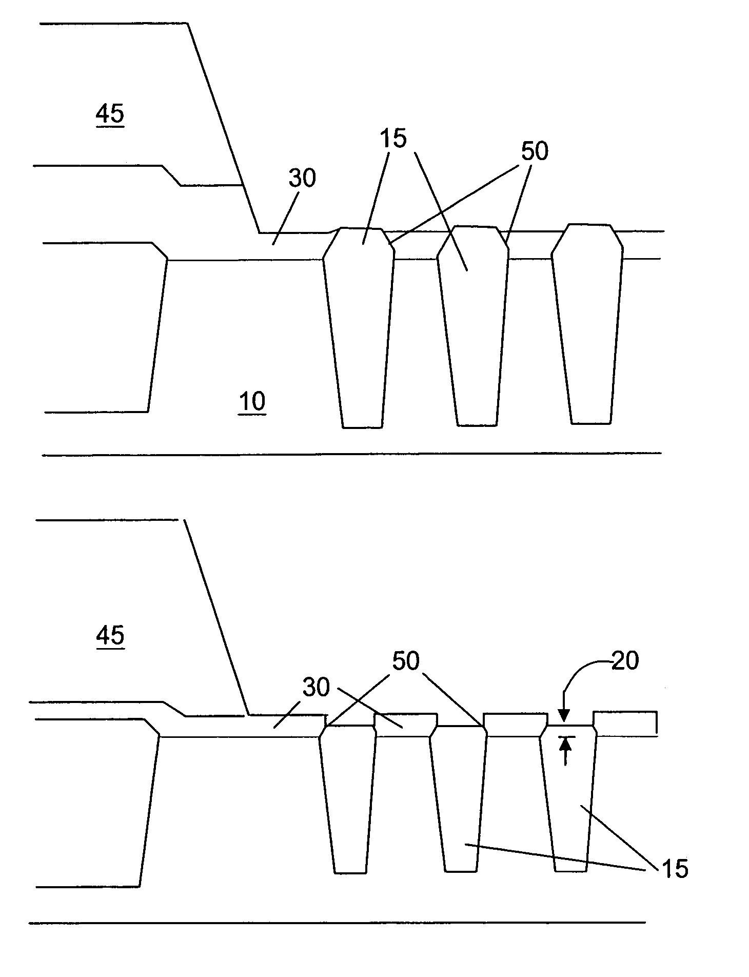
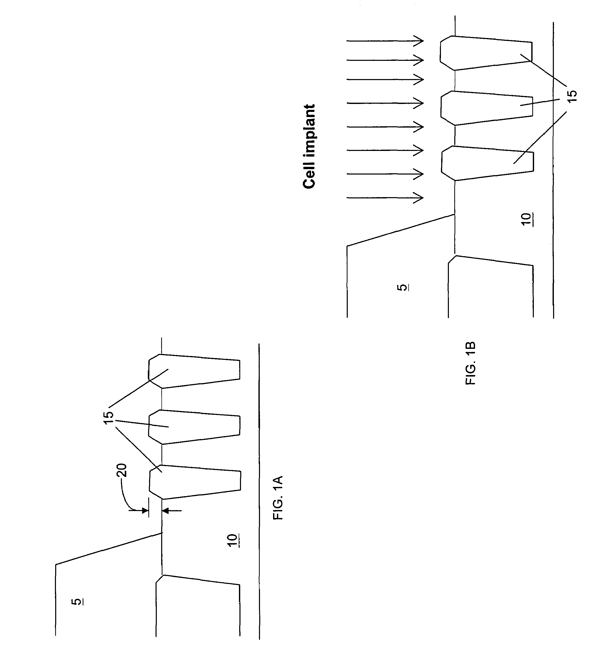
[0007]In some embodiments, a method comprises the steps of providing a semiconductor substrate having regions isolated from each other by shallow trench isolation (STI) structures protruding above a surface of the substrate by a step height; forming a bottom antireflective coating (BARC) layer overlying the surface of the substrate and the STI structures; etching back a portion of the BARC layer overlying at least one of the STI structures, and partially etching back the at least one STI structure, to reduce the step height by which the STI structure protrudes above the surface of the substrate; and removing a remaining portion of the BARC layer between adjacent STI structures

Problems solved by technology

Using EEPROM devices in circuitry permits in-circuit erasing and reprogramming of the device, a feat not possible with conventional EPROM memory.
Such erase operations can cause operation of flash memory devices and the devices themselves to be susceptible to extrinsic defects, introduced in the fabrication process.

Method used


Image

  • Process to improve programming of memory cells
  • Process to improve programming of memory cells
  • Process to improve programming of memory cells

Examples


Embodiment Construction

[0012]This description of the exemplary embodiments is intended to be read in connection with the accompanying drawings, which are to be considered part of the entire written description. In the description, relative terms such as “lower,”“upper,”“horizontal,”“vertical,”“above,”“below,”“up,”“down,”“top” and “bottom” as well as derivative thereof (e.g., “horizontally,”“downwardly,”“upwardly,” etc.) should be construed to refer to the orientation as then described or as shown in the drawing under discussion. These relative terms are for convenience of description and do not require that the apparatus be constructed or operated in a particular orientation. Terms concerning attachments, coupling and the like, such as “connected” and “interconnected,” refer to a relationship wherein structures are secured or attached to one another either directly or indirectly through intervening structures, as well as both movable or rigid attachments or relationships, unless expressly described otherw...


PUM


Abstract

A method is provided for fabrication of a semiconductor substrate having regions isolated from each other by shallow trench isolation (STI) structures protruding above a surface of the substrate by a step height. The method includes the steps of forming a bottom antireflective coating (BARC) layer overlying the surface of a semiconductor substrate and the surface of STI structures; etching back a portion of the BARC layer overlying at least one of the STI structures, and partially etching back the at least one of the STI structures, to reduce the step height by which the STI structure protrudes above the surface of the substrate; and removing a remaining portion of the BARC layer between adjacent STI structures. The method may be used to fabricate semiconductor devices including memory cells that have improved reliability.

Description

FIELD OF THE INVENTION[0001]The present invention relates generally to a fabrication method for semiconductor devices. More particularly, the present invention relates to a fabrication method for memory cells.BACKGROUND[0002]Integrating different devices, such as the memory cell and the logic circuit on the same wafer has become a trend in the semiconductor industry. This has provided portable electronic devices such as digital cameras, notebooks, personal digital assistants (PDA), mobile phones, and the like. All of these devices need a dependable and convenient method to maintain their information and / or data for substantial periods of time without refresh cycles and / or power—non-volatile memory. A widely utilized type of non-volatile memory device is flash memory. Flash memory devices achieve relatively high speeds of operation and are able to maintain their data without power and / or refresh cycles.[0003]A few examples of non-volatile semiconductor memory include read only memory...

Claims


Application Information

Patent Timeline
Patent Type & Authority Patents(United States)
IPC IPC(8): H01L21/762
CPCH01L27/11521H01L21/76224H01L27/10894H01L27/11H10B12/09H10B10/00H10B41/30
Inventor LIU, SHIH-CHANGCHU, WEN-TINGKU, CHIEN-MINGLO, CHI-HSINTSAI, CHIA-SHIUNGHSIEH, CHIA-TA
Owner TAIWAN SEMICON MFG CO LTD
Why Eureka
Try Eureka