Method of reducing step height

a technology of step height and step height, which is applied in the direction of semiconductor/solid-state device manufacturing, basic electric elements, electric apparatus, etc., can solve the problems of negative affecting process yield and electrical performance of devices, negative affecting etc., to improve process yield and electrical performance, reduce step height, and reduce the effect of step heigh

Inactive Publication Date: 2005-09-15
VANGUARD INTERNATIONAL SEMICONDUCTOR CORPORATION
View PDF2 Cites 6 Cited by
  • Summary
  • Abstract
  • Description
  • Claims
  • Application Information

AI Technical Summary

Benefits of technology

[0011] Thus, the main object of the present invention is to provide a method of reducing step height, providing the minimum step height when forming high-voltage and low-voltage device areas on a substrate, in order to improve process yield and electrical performance.
[0012] In order to achieve the described objects, the present invention provides a method of reducing step height. First, a substrate, comprising a low-voltage device area and high-voltage device area divided by an isolation structure, is provided. The substrate further comprises a pad oxide layer on the surface of the low-voltage device area and high-voltage device area. Then, a silicon nitride layer and patterned mask layer are sequentially formed overlying the substrate. Silicon nitride layer thickness is at least about 500 Å thick. The patterned mask layer exposes the silicon nitride layer in the high-voltage device area and parts of the isolation structure adjacent thereto. Next, the exposed silicon nitride layer is anisotropically etched using the mask layer, exposing the high-voltage device area and parts of the isolation structure. Next, the patterned mask layer and pad oxide on the surface of the high-voltage device area are sequentially removed. Next, a first oxide layer is formed on the exposed high-voltage device area and isolation structure using the silicon nitride layer as a mask. Further, the remaining silicon nitride layer and pad oxide layer on the surface of the low-voltage device area are sequentially removed. Finally, a second oxide layer, thinner than the first oxide layer, is formed on the low-voltage device layer.

Problems solved by technology

Therefore, as shown in FIG. 1E, when a polycrystalline silicon layer 160 formed on the substrate 100 is patterned in subsequent gate forming process, polycrystalline silicon spacers 161 usually remain on high sidewalls, negatively affecting the process yield and electrical performance of the devices.
The ONO layer 40, acting as the hard mask of low-voltage device area, is usually about 100 to 500 Å thick and cannot be made thicker due to its role as the dielectric layer of the capacitor in the gate of the flash memory cell in memory cell area A. Oxygen may penetrate the ONO layer 40 on the low-voltage device area B as a result of insufficient thickness during the formation of the first gate oxide layer 22 about 1000 to 2000 Å when desired, resulting in formation of an unwanted oxide layer between substrate 10 and ONO layer 40, thereby negatively affecting process yield and electrical performance.

Method used


Image

  • Method of reducing step height
  • Method of reducing step height
  • Method of reducing step height

Examples


Embodiment Construction

[0018] The following embodiments are intended to illustrate the invention more fully without limiting the scope of the claims, since numerous modifications and variations will be apparent to those skilled in this art.

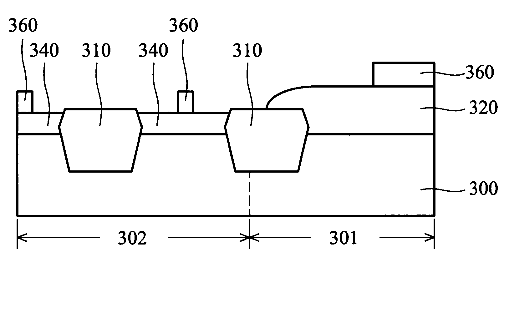
[0019]FIGS. 3A through 3E are cross-sections of a method of reducing step height of the present invention.

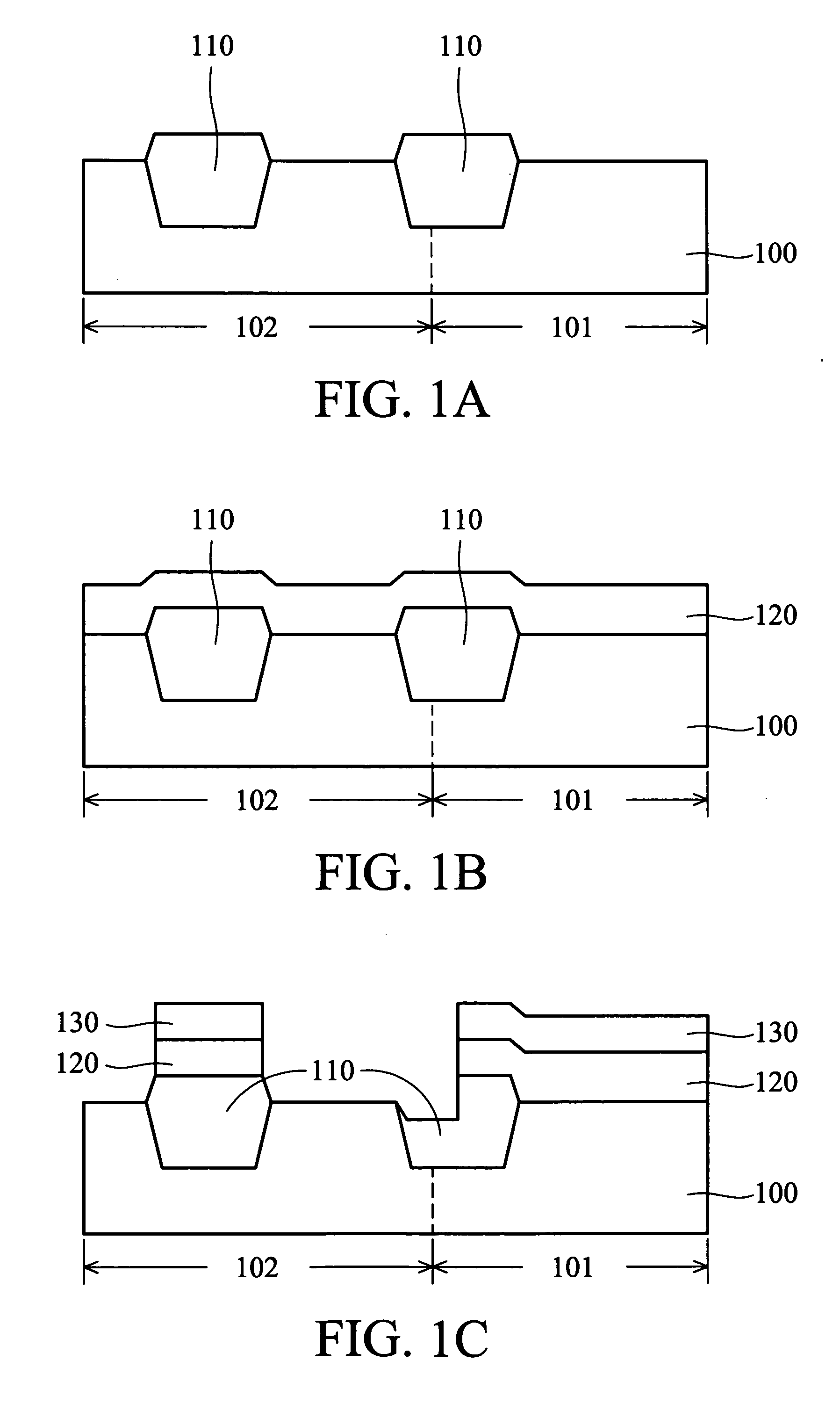
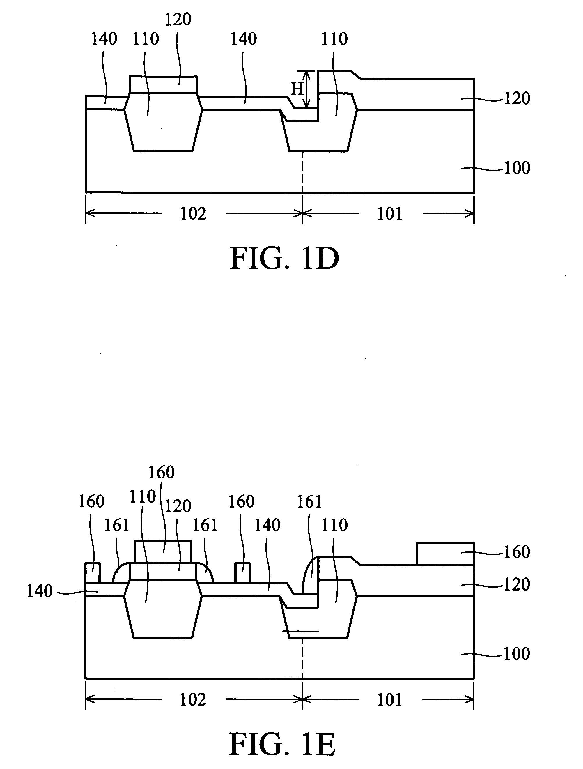
[0020] In FIG. 3A, a substrate 300, usually single-crystalline silicon, is provided. The substrate 300 is usually covered by a pad oxide layer 303 on a surface. The substrate 300 comprises a high-voltage device area 301 and low-voltage device area 302 divided by an isolation structure 310. The isolation structure 310 can be a shallow trench isolation (STI) structure or field oxide (FOX) layer. In this embodiment, the pad oxide layer 303 is approximately 200 Å thick, and the isolation structure 310 is STI, and usually an oxide layer.

[0021] In FIG. 3B, a silicon nitride layer 350, preferably as thick as 500 Å or more, is formed on substrate 300, subsequently acting...


PUM


Abstract

A method of reducing substrate step height. The method includes providing a substrate having a low-voltage device area and high-voltage device area divided by an isolation structure, forming an oxidation mask at least approximately 500 Å thick over the low-voltage device area and parts of the isolation structure, forming a first oxide layer on the exposed high-voltage device area and isolation structure using the oxidation mask as a mask, removing the oxidation mask, and forming a second oxide layer, thinner than the first oxide layer, on the low-voltage device layer.

Description

BACKGROUND OF THE INVENTION [0001] 1. Field of the Invention [0002] The present invention relates to a semiconductor process, and more specifically to a method of reducing step height when forming high-voltage and low-voltage device areas on a substrate. [0003] 2. Description of the Related Art [0004]FIGS. 1A through 1E are cross-sections of a conventional process forming high-voltage and low-voltage device areas. The substrate 100 in FIG. 1A has a high-voltage area 101 and low-voltage area 102 divided by a shallow trench isolation (STI) structure 110. [0005] In FIG. 1B, an oxide layer 120 about 1000 to 2000 Å thick is formed on the substrate 100. In FIG. 1C, a patterned mask layer 130 is formed on the oxide layer 120. The oxide layer 120 on the low-voltage device area 101 is removed using the patterned mask layer 130 as an etch mask, leaving that on the high-voltage device area 102 to act as gate oxide. Further, over-etching is usually performed to ensure complete removal of the ox...

Claims


Application Information

Patent Timeline
Patent Type & Authority Applications(United States)
IPC IPC(8): H01L21/336H01L21/8234
CPCH01L21/28123H01L21/823481H01L21/823462
Inventor YANG, JIA-WEICHANG, DA-PONG
Owner VANGUARD INTERNATIONAL SEMICONDUCTOR CORPORATION
Why Eureka
Try Eureka