Method and system for implementing timing aware metal fill

a technology of timing awareness and metal filling, applied in the field of integrated circuit design and manufacture, can solve the problems of reducing yield and impact circuit performance affecting the performance of the circuit, etc., and achieves the effects of reducing free space available, avoiding harmful capacitance effects, and avoiding or minimizing cross-capacitance problems

Inactive Publication Date: 2012-04-17
CADENCE DESIGN SYST INC
View PDF12 Cites 10 Cited by
  • Summary
  • Abstract
  • Description
  • Claims
  • Application Information

AI Technical Summary

Benefits of technology

[0002]In recent years, in integrated circuit (IC) manufacturing, chemical-mechanical polishing (CMP) has emerged as an important technique for planarizing dielectrics because of its effectiveness in reducing local step height and achieving a measure of global planarization not normally possible with spin-on and resist etch back techniques. However, CMP processes have been hampered by layout pattern dependent variation in the inter-level dielectric (ILD) thickness which can reduce yield and impact circuit performance.
[0003]Metal-fill patterning is a common approach for reducing layout pattern dependent dielectric thickness variation. Metal-fill patterning is the process of filling large open areas on each metal layer with a metal pattern to compensate for pattern-driven variations. The manufacturer of the chip normally specifies a minimum and maximum range of metal that should be present at each portion of the die. If there is an insufficient amount of metal at a particular portion on the chip, then metal-fill is used to increase the proportion of metal in that portion. However, too much metal may cause dishing to occur. Therefore, the metal-fill process should not cause the die to exceed any specified maximum range of metal for the chip.
[0006]Another solution is to place metal fill farther away from existing objects in the layout. A metal fill tool may use spacing rules when inserting metal fill, which mandate that metal fill cannot be inserted within a specified distance around existing shapes. These rules are uniformly applied for all shapes in the design. In an attempt to avoid harmful capacitance effects, organizations may increase the mandated spacing distance so that the actual spacing distance between metal fill and existing shapes exceeds what is required by the spacing rules. For instance, if the spacing rules require a distance of x, then organizations may actually use a spacing distance of 2× to avoid timing problems. The problem is that this approach of trying to put extra space around every object will significantly restrict the free space available to place metal fill, thereby preventing metal fill tools from hitting density targets for the fill.
[0007]Therefore, there is a need for an improved approach for implementing metal fill on an electrical device without causing creating cross-coupling capacitance problems. In some embodiments of the invention, timing aware metal fill insertion is performed to avoid or minimize cross-capacitance problems on the IC design. A cost may be assigned to different candidate metal fill shapes. The cost is associated with the expected effect upon timing requirements by the metal fill shape, with lower costs corresponding to lower expected impacts upon the timing requirements. To meet density requirements, lower cost metal fill shapes are inserted prior to higher cost metal fill shapes.

Problems solved by technology

However, CMP processes have been hampered by layout pattern dependent variation in the inter-level dielectric (ILD) thickness which can reduce yield and impact circuit performance.
However, too much metal may cause dishing to occur.
The addition of the metal fill may negatively affect the electrical performance of the integrated circuit device.
In particular, placement of metal fill shapes near existing features on the IC may cause cross coupling capacitances to occur on the device.
As timing closure is a critical goal in the design of high speed devices, additional cross coupling capacitances can cause additional iterations in the design process due to slowing down some signals.
The problem with that lack of consistency is that there will be more OCV (On Chip Variation) issues as the wiring in higher density areas will become thinner than in the lower density areas.
This difference in thickness is very difficult to account for.
The problem is that this approach of trying to put extra space around every object will significantly restrict the free space available to place metal fill, thereby preventing metal fill tools from hitting density targets for the fill.

Method used


Image

  • Method and system for implementing timing aware metal fill
  • Method and system for implementing timing aware metal fill
  • Method and system for implementing timing aware metal fill

Examples


Embodiment Construction

[0018]Disclosed is an improved method and system for implementing metal fill for an integrated circuit design which is capable of achieving the preferred density levels while minimizing cross coupling capacitance, effects.

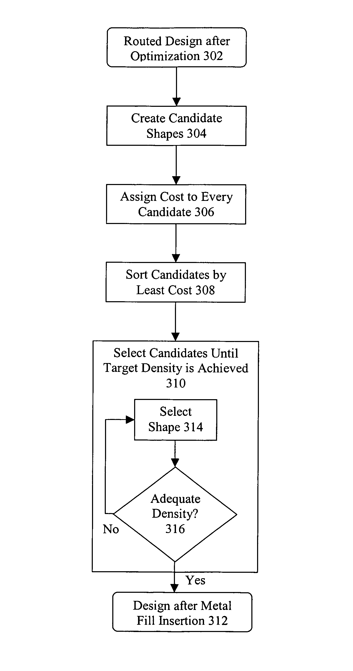
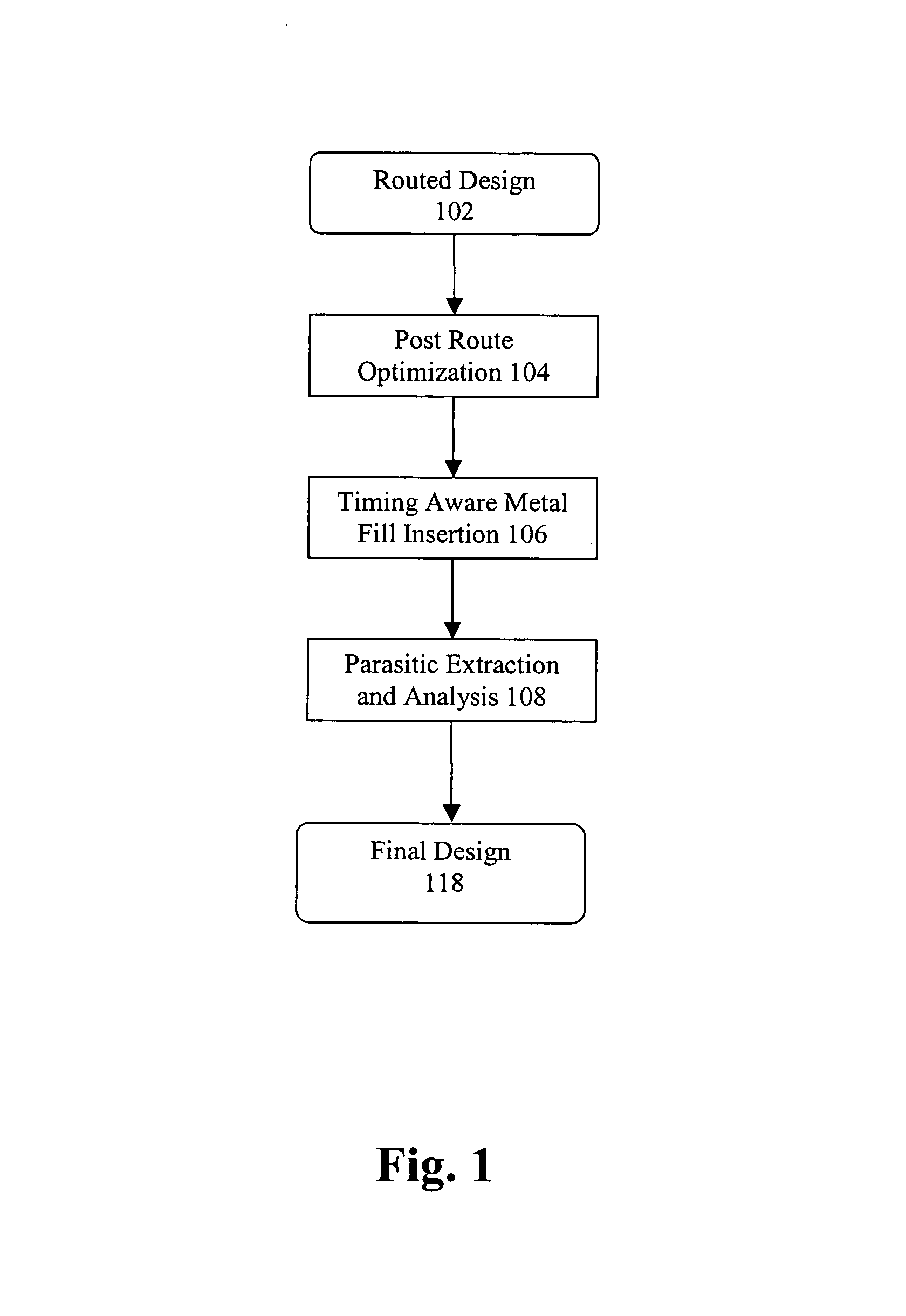
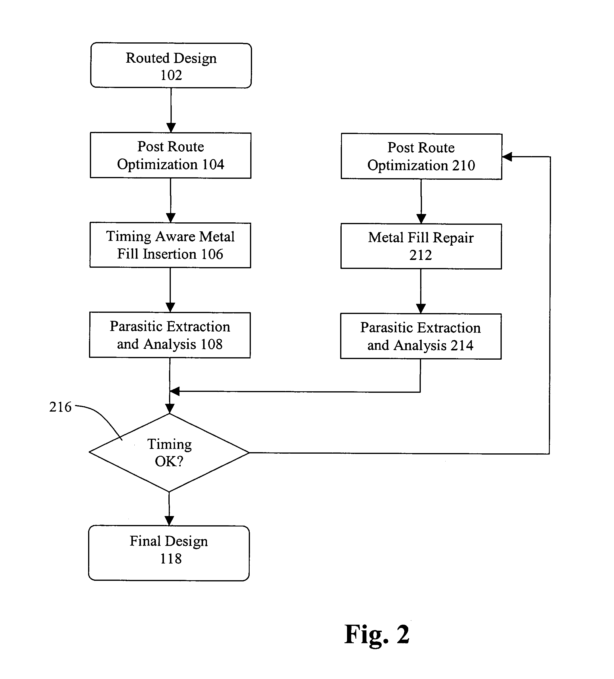
[0019]FIG. 1 shows a process for implementing metal fill according to some embodiments of the invention. The use of this invention will increase the likelihood that the required timing for the device will be met in one pass, preventing the extra iteration(s) of metal fill insertion.

[0020]At 102, the IC design is placed and routed to generate a routed design. Any suitable approach can be taken to place and route the IC design. At 104, post route optimization is performed against the design. For example, compaction techniques may be used to optimize the layout of the IC design.

[0021]At 106, a one pass approach is taken to perform timing aware metal fill insertion into the layout. The one-pass approach permits metal fill to be inserted into the IC design in a manner t...


PUM


Abstract

An improved approach for implementing metal fill on an electrical device without causing creating cross-coupling capacitance problems is disclosed. Timing aware metal fill insertion is performed to avoid or minimize cross-capacitance problems on the IC design. A cost may be assigned to different candidate metal fill shapes. The cost is associated with the expected effect upon timing requirements by the metal fill shape, with lower costs corresponding to lower expected impacts upon the timing requirements. To meet density requirements, lower cost metal fill shapes are inserted prior to higher cost metal fill shapes.

Description

BACKGROUND AND SUMMARY[0001]The invention relates to the design and manufacture of integrated circuits, and more particularly, to techniques, systems, and methods for implementing metal-fill on an integrated circuit.[0002]In recent years, in integrated circuit (IC) manufacturing, chemical-mechanical polishing (CMP) has emerged as an important technique for planarizing dielectrics because of its effectiveness in reducing local step height and achieving a measure of global planarization not normally possible with spin-on and resist etch back techniques. However, CMP processes have been hampered by layout pattern dependent variation in the inter-level dielectric (ILD) thickness which can reduce yield and impact circuit performance.[0003]Metal-fill patterning is a common approach for reducing layout pattern dependent dielectric thickness variation. Metal-fill patterning is the process of filling large open areas on each metal layer with a metal pattern to compensate for pattern-driven v...

Claims


Application Information

Patent Timeline
Patent Type & Authority Patents(United States)
IPC IPC(8): G06F17/50
CPCH01L23/522G06F17/5081G06F2217/12H01L2924/0002H01L2924/00Y02P90/265G06F30/398G06F2119/18Y02P90/02
Inventor NOICE, DAVIDNUNN, GARYSEO, INHWANKAO, WILLIAMDONG, XIAOPENG
Owner CADENCE DESIGN SYST INC
Why Eureka
Try Eureka