Recovery processing method of an electrode

a recovery processing and electrode technology, applied in the field of recovery processing methods of electrodes, can solve the problems of easy breaking of oxide films, wear of micro-patterns or ceramic spray coatings having wear resistance, and limitations in the life of durability, so as to achieve the effect of easy and assured formation

Inactive Publication Date: 2007-01-09
YAMAICHI ELECTRONICS
View PDF11 Cites 18 Cited by
  • Summary
  • Abstract
  • Description
  • Claims
  • Application Information

AI Technical Summary

Benefits of technology

[0008]In view of the above problems, the present invention has been made to provide a recovery processing method of an electrode for recovering a connection surface of an electrode section in an electrode plate to be electrically connected to a terminal of a semiconductor device so that the connection surface is recovered to have a predetermined surface roughness, which the method is capable of easily and reliably forming a predetermined irregularity on the connection surface of the electrode section in the worn electrode plate.
[0017]As apparent from the above description, according to the recovery processing method of an electrode, since the transfer plate and the electrode plate are heated at the predetermined temperature for the predetermined period toward the connection surface of the electrode section while pressing the transfer plate placed on the connection surface of the electrode section toward the connection surface of the electrode section at the predetermined pressure, both the plates relatively slide to each other due to the difference in the expansion, it is possible to scrape the connection surface of the electrode to have the predetermined surface roughness and thus easily and assuredly form the predetermined irregularity on the worn connection surface of the electrode section in the electrode plate.

Problems solved by technology

Thus, the micro-projections have an effect of easily breaking the oxide film.
In the above-mentioned IC socket for the electronic equipment, when the electric contact section in the conductive pattern has been repeatedly used, the micro-pattern or the ceramic sprayed coating having wear resistance is also worn due to the contact pressure or the like because a life of the durability has a certain limitations.
Accordingly, the electric contact section or the end surface of the conductive path becomes gradually non-irregularity flat surface rather than recovery as the frequency of use increases, which may increases the contact area to result in an insufficient contact pressure.
Thus, there may be a case in that the original reliable electric connection is not obtainable as repeating the use thereof.

Method used


Image

  • Recovery processing method of an electrode
  • Recovery processing method of an electrode
  • Recovery processing method of an electrode

Examples


first embodiment

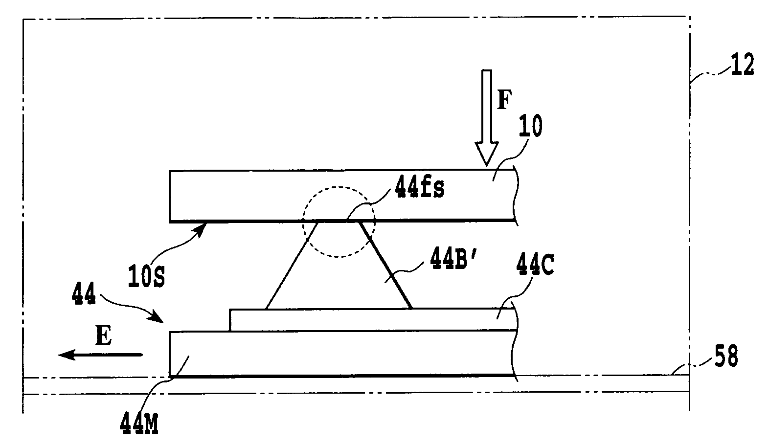
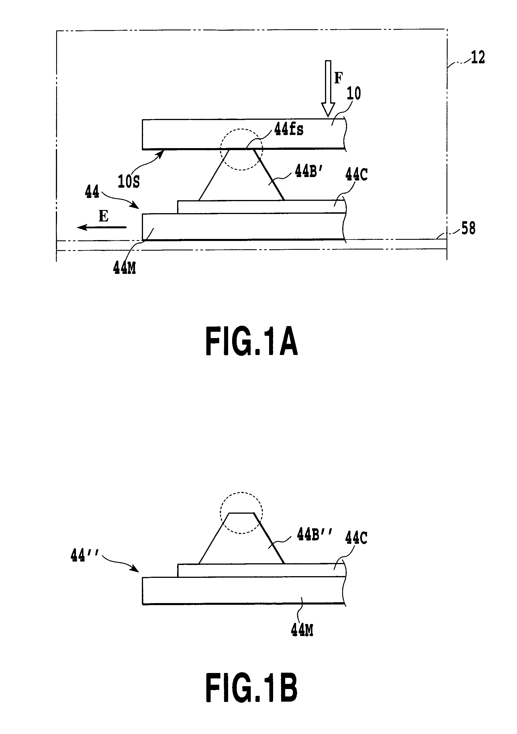
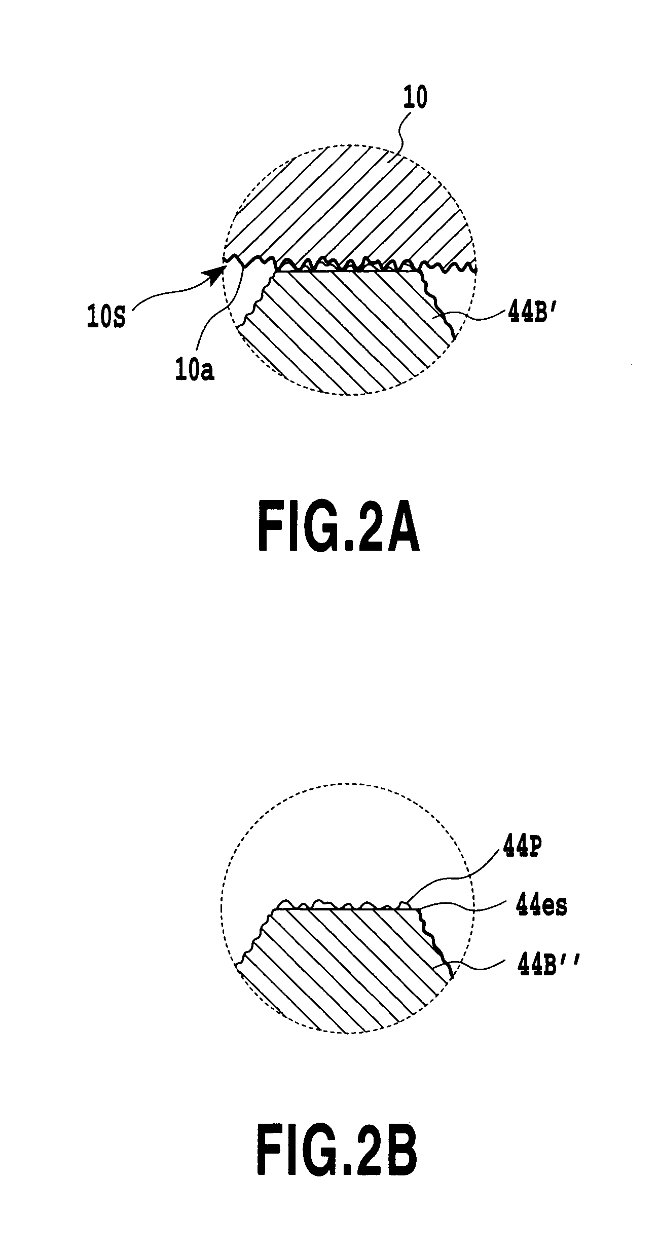
[0080]To solve such a problem, according to a recovery processing method of an electrode according to the present invention, a transfer plate 10 having a predetermined thickness is prepared as shown in FIG. 1A. The transfer plate 10 is made of cold tool steel (Japanese Industrial standards mark SKS, SKD) plated with chromium as a surface treatment (having a coefficient of linear expansion of approximately 11.5×10⁻⁶ / ° C.), and has irregularity of a predetermined roughness on at least one transfer surface 10s as enlargedly shown in FIG. 2A.

[0081]First, the contact sheet 44, of which the bump 44B′ is worn, is disposed as shown in FIG. 1A, and the above-mentioned carrier unit 40 on which is mounted the transfer plate 10 in place of the bare chip 60 is arranged in a constant temperature bath 12 for maintaining the room temperature at a predetermined value. The constant temperature bath 12 is provided with a temperature regulator capable of variously adjusting the room temperature.

[0082]A...

second embodiment

[0096]FIGS. 10A, 10B and 10C schematically illustrate the respective steps in a recovery processing method of an electrode according to the present invention.

[0097]A contact sheet 80 used in the embodiment shown in FIGS. 10A to 10C has a plurality of bumps 84B arranged in a substrate 84M in correspondence to an electrode group of a bare chip 60 to be electrically connected thereto as shown in FIG. 10A. A tip end of the respective bump 84B is projected at a predetermined height from the surface of the substrate 84M. A micro-irregularity 84a is formed over the entirety of the surface of the tip end thereof as shown in FIG. 11A in an enlarged scale.

[0098]The respective bump 84B is electrically connected to a pad (not shown) via a conductive layer 84C formed of copper foil. The pad is formed at each of the opposite ends of the substrate 84M projected from each of the opposite ends of the base member 42. The respective bump 84B is formed of material in which gold (having Knoop hardness i...

third embodiment

[0130]FIGS. 15 and 16 illustrate a carrier unit stage together with a transfer plate fixing bead used in a recovery processing method of an electrode according to the present invention.

[0131]In this regard, in FIGS. 15 and 16, the same reference numerals are used for denoting the same elements in FIGS. 7 and 8, and the explanation thereof will be eliminated. Also, in FIGS. 15 and 16, a state is illustrated in which part of constituent elements of the carrier unit are held in the carrier unit stage while the pressing covering is removed.

[0132]As part of the carrier unit is shown in FIGS. 15 and 17, the carrier unit includes a carrier housing 116 having an accommodation portion 116A for receiving a bare chip 60, the contact sheet 44 placed via an elastic sheet 110 on a base member 108 forming a bottom of the accommodation portion 116A of the carrier housing 116, a pressing covering (not shown) having a press body for pressing an electrode group of the bare chip 60 to bumps 44B in the ...


PUM

PropertyMeasurementUnit
Raaaaaaaaaaa
temperatureaaaaaaaaaa
thicknessaaaaaaaaaa

Abstract

While a transfer surface 10a of a transfer plate 10 having a predetermined surface roughness is brought into contact with a plurality of bumps 44B on a contact sheet 44 formed on a substrate 44M having the coefficient of linear expansion larger than that of the transfer plate 10 at a predetermined pressure, the substrate 44M and the transfer plate 10 are heated to a predetermined temperature to recover the surface roughness of the bump 44B to a predetermined value.

Description

[0001]This application is a continuation-in-part of U.S. application Ser. No. 10 / 443,813 filed May 23, 2003 now U.S. Pat. No. 6,905,952. Accordingly, this application claims priority benefit to U.S. application Ser. No. 10 / 443,813, and also claims priority benefit to Japanese Patent Application No. 2002-153062 filed May 27, 2002, and Japanese Patent Application No. 2003-003508 filed Jan. 9, 2003, and further, Japanese Patent Application No. 2004-342991 filed Nov. 26, 2004, and the contents of each of the aforementioned U.S. application and Japanese Applications are incorporated hereinto by reference.BACKGROUND OF THE INVENTION[0002]1. Field of the Invention[0003]The present invention relates to a recovery processing method of an electrode for recovering a connection surface of an electrode region in an electrode plate for electrically connecting the same to terminals of a semiconductor device, to have a predetermined surface roughness.[0004]2. Description of the Related Art[0005]Gen...

Claims


Application Information

Patent Timeline
Patent Type & Authority Patents(United States)
IPC IPC(8): B23P6/00H01R13/22H01R13/53H01R43/00H01R43/16H05K3/00H05K3/40
CPCH01R13/22H05K3/4007H01R43/002Y10T29/49204H05K2201/0367H05K2203/0278H05K2203/0307H05K2203/1152Y10T29/49002Y10T29/49725Y10T29/49147Y10T29/49218Y10T29/49151Y10T29/49117Y10T29/49718Y10T29/49208
Inventor SUZUKI, TAKEYUKIWAKABAYASHI, YOSHINORI
Owner YAMAICHI ELECTRONICS
Why Eureka
Try Eureka