Removable ESD protection device using diodes

a protection device and diode technology, applied in the field of reusable devices, can solve the problems of physical damage to the sensors, spurious discharge of static electricity, and buildup of electrostatic charges on the various elements

Inactive Publication Date: 2007-01-09
INT BUSINESS MASCH CORP
View PDF23 Cites 15 Cited by
  • Summary
  • Abstract
  • Description
  • Claims
  • Application Information

AI Technical Summary

Benefits of technology

[0018]The present invention provides a reusable device for protecting an electronic component from ESD / EOS damage. The protective device includes a substrate having one or more coupling regions that are adapted for detachable coupling to a cable and / or another device, e.g., a card, the electronic component (an element of a magnetic tape or disk head, etc.), etc. In this way, the device may be interposed between a testing system and the electronic component being tested. One or more diodes are coupled to the substrate. Contact leads are coupled to the coupling region of the substrate, and are in electrical communication with the diode(s). The diode(s) provide current shunting in the event of an ESD shock or other power surge, thereby protecting the electronic component from damage.
[0019]The substrate may be flexible to reduce stress on any cables to which it is attached. The substrate may also be substantially resilient for ease of manufacture and / or for durability to extend its useful life.
[0021]Preferably, a compression fitting is used to couple the coupling region of the substrate to the cable or other device. The compression fitting allows rapid connection and removal of the of the device to cables and boards while providing reliable electrical coupling.

Problems solved by technology

A major problem that is encountered during manufacturing, handling and use of magnetic recording transducers, referred to as heads, is the buildup of electrostatic charges on the various elements of a head or other objects which come into contact with the heads, particularly heads of the thin film type, and the accompanying spurious discharge of the static electricity thus generated.
These static charges may be discharged through the head causing excessive heating of the sensitive sensors which result in physical damage to the sensors.
As described above, when a head is exposed to electrostatic discharge (ESD), or even a voltage or current input larger than that intended under normal operating conditions, referred to as electrical overstress or EOS, the sensor and other parts of the head may be damaged.
This sensitivity to electrical damage is particularly severe for MR read sensors because of their relatively small physical size.
Discharge currents of tens of milliamps through such a small resistor can cause severe damage or completely destruction of the MR sensor.
The nature of the damage which may be experienced by an MR sensor varies significantly, including complete destruction of the sensor via melting and evaporation, oxidation of materials at the air bearing surface (ABS), generation of shorts via electrical breakdown, and milder forms of magnetic or physical damage in which the head performance may be degraded.
The large number of MR sensors in a tape drive, and thus, the significantly higher cost, makes testing during manufacturing more important and ESD loss due to a single element is very expensive as the entire head must then be scrapped.
However, both of these approaches have significant disadvantages.
This leaking current through the diode leads to noise, which will lower the signal to noise ratio of the readback process.
Diodes also introduce parasitic capacitance across the head, and from the head leads to the electrical ground, which adversely affects the maximum readback bandwidth achievable with the head.
The problem with this technique is that it is no longer possible to test the head after the short is applied.
However, since it is sometimes necessary to measure the resistance or other parameters of the device during fabrication, the shorting device must be removed, exposing the device to possible ESD / EOS damage.
However, this method is difficult to realize, as switches require large amounts of real estate on the back of the slider, and the switching process requires low resistance shorting and re-shorting structures.
Since modem tape heads have multiple read elements, it can be expensive to add diodes to each cable, particularly where the head and cable are scrapped during the testing phase.
While mounting disposable diodes on a single slider may be cost effective, the shear number of diodes required for a modem tape head adds significant cost to the head if the diodes are not reusable by multiple heads during manufacturing.
Furthermore, the added weight of many diodes or chips on the cable will affect the dynamics of the head actuation, potentially degrading its track following performance.

Method used


Image

  • Removable ESD protection device using diodes
  • Removable ESD protection device using diodes
  • Removable ESD protection device using diodes

Examples


Embodiment Construction

[0039]The following description is the best embodiment presently contemplated for carrying out the present invention. This description is made for the purpose of illustrating the general principles of the present invention and is not meant to limit the inventive concepts claimed herein.

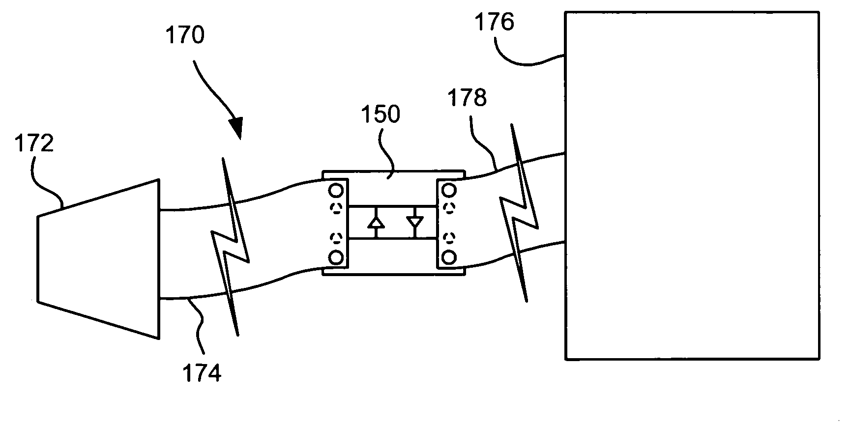
[0040]For purposes of fabricating and assuring quality of certain types of electronic devices, it is desirable to perform tests at various stages in the manufacturing process. The present description discloses a protective device for protecting delicate components of the electronic device from ESD and EOS damage. More particularly, this invention discloses a removable protective device which can be used during manufacturing and removed when the electronic device is installed in the end device. The protective device can then be reused.

[0041]Although the invention is described as embodied for use with a magnetic tape storage system, the invention also applies to other electronic devices, including magne...


PUM

PropertyMeasurementUnit
response timeaaaaaaaaaa
heightaaaaaaaaaa
heightaaaaaaaaaa

Abstract

A removable device which is used during manufacturing for ESD / EOD protection and removed when the head is mounted in a drive. The device consists of crossed diodes which are mounted in the device and will connect to the readers. Each reader has two or more crossed diodes detachably coupled to its leads. The diodes are mounted on a device which is removable at the end of manufacturing assembly and the device can be reused. The device limits the voltage across a reader to the voltage limit of the number of diodes connected in series. Crossed diodes are connected in parallel with the electrical device to be protected to protect against random current spikes in either direction through the device in question. The device has leads which can be connected to an external device to measure the reader resistance or other electrical properties.

Description

FIELD OF THE INVENTION[0001]The present invention relates to a device for protection from electrostatic discharge and electrical overstress, and more particularly, this invention relates to a reusable device for protecting an electronic device from electrostatic discharge and electrical overstress.BACKGROUND OF THE INVENTION[0002]Magnetic head-based systems have been widely accepted in the computer industry as a cost-effective form of data storage. In a magnetic disk drive system, a magnetic recording medium in the form of a disk rotates at high speed while a magnetic read / write transducer, referred to as a magnetic head, “flies” slightly above the surface of the rotating disk. The magnetic disk is rotated by means of a spindle drive motor. The magnetic head is attached to or formed integrally with a “slider” which is suspended over the disk on a spring-loaded support arm known as the actuator arm. As the magnetic disk rotates at operating speed, the moving air generated by the rota...

Claims


Application Information

Patent Timeline
Patent Type & Authority Patents(United States)
IPC IPC(8): G11B5/39G11B5/40G11B5/127G11B5/33G11B5/49G11B33/14
CPCG11B33/1493G11B5/4915
Inventor IBEN, ICKO E. T.
Owner INT BUSINESS MASCH CORP
Why Eureka
Try Eureka