Semiconductor component and method of manufacture

a technology of semiconductor components and resistors, applied in the direction of resistors, semiconductor devices, electrical equipment, etc., can solve the problems of low fixed resistance value, unacceptably slow device, and voltage drop across the resistor too low to provide adequate esd protection for the semiconductor devi

Inactive Publication Date: 2007-01-16
GLOBALFOUNDRIES INC
View PDF26 Cites 15 Cited by
  • Summary
  • Abstract
  • Description
  • Claims
  • Application Information

AI Technical Summary

Benefits of technology

[0005]The present invention satisfies the foregoing need by providing a semiconductor component having a tuned variable resistance resistor and methods for manufacturing the semiconductor component. In accordance with one aspect, the present invention comprises a method for manufacturing a semiconductor component hardened to a transient electrical signal. The method includes providing a semiconductor substrate having a semiconductor device formed therefrom, wherein the semiconductor device has a device node. A first input / output node is coupled to the device node via a tuned variable resistance resistor.
[0006]In accordance with another aspect, the present invention comprises a method for protecting a semiconductor component from a transient electrical signal by coupling a tuned dynamic resistance to at least one device. The tuned dynamic resistance operates at its saturation current during an electrostatic discharge event.
[0007]In accordance with another aspect, the present invention comprises a semiconductor component having an input / output node coupled to a device node via a tuned dynamic resistance. The length of the tuned dynamic resistance is selected so that it can carry a predetermined stress current and develop a predetermined voltage thereacross in the event of a transient electrical stimulus.

Problems solved by technology

A drawback of including this resistor is that it has a fixed resistance value that must be kept low for use in high frequency or radio frequency applications.
If the resistance value is too high, the Resistance-Capacitance (RC) time constant of the pin coupled to the bond pad makes the device unacceptably slow.
However, when the resistance is too low, the voltage drop across the resistor is too low to provide adequate ESD protection for the semiconductor device.

Method used


Image

  • Semiconductor component and method of manufacture
  • Semiconductor component and method of manufacture
  • Semiconductor component and method of manufacture

Examples


Embodiment Construction

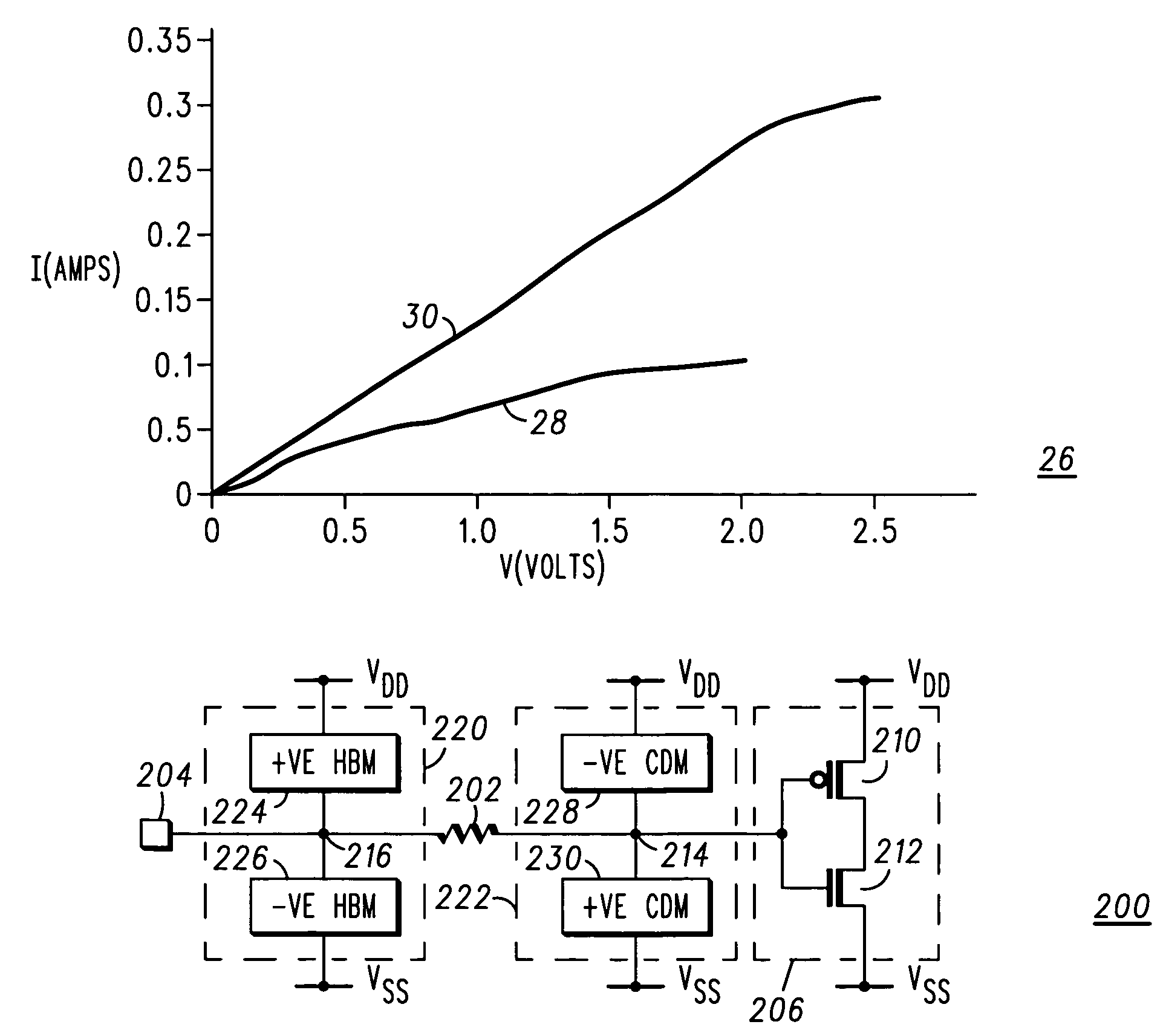
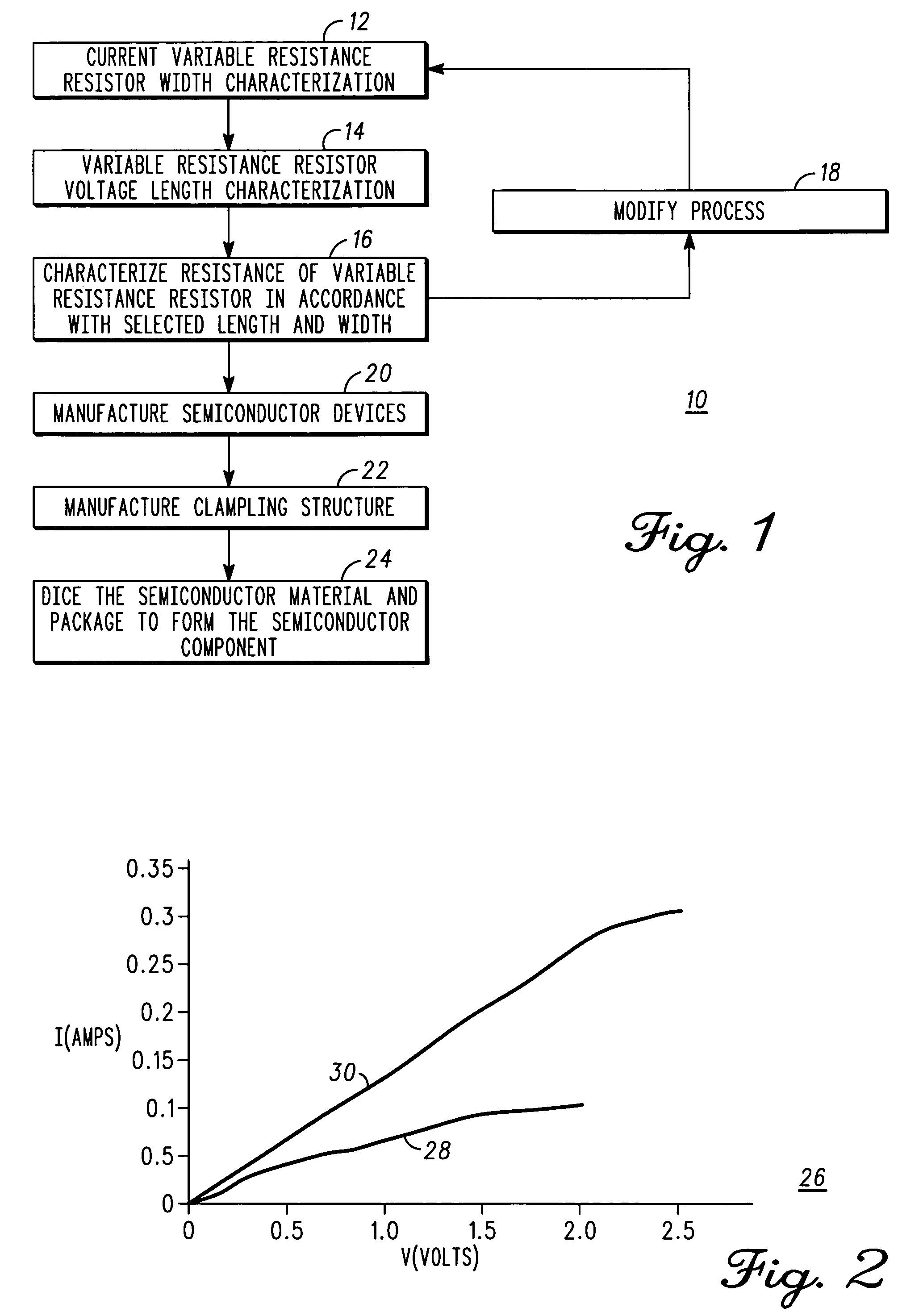
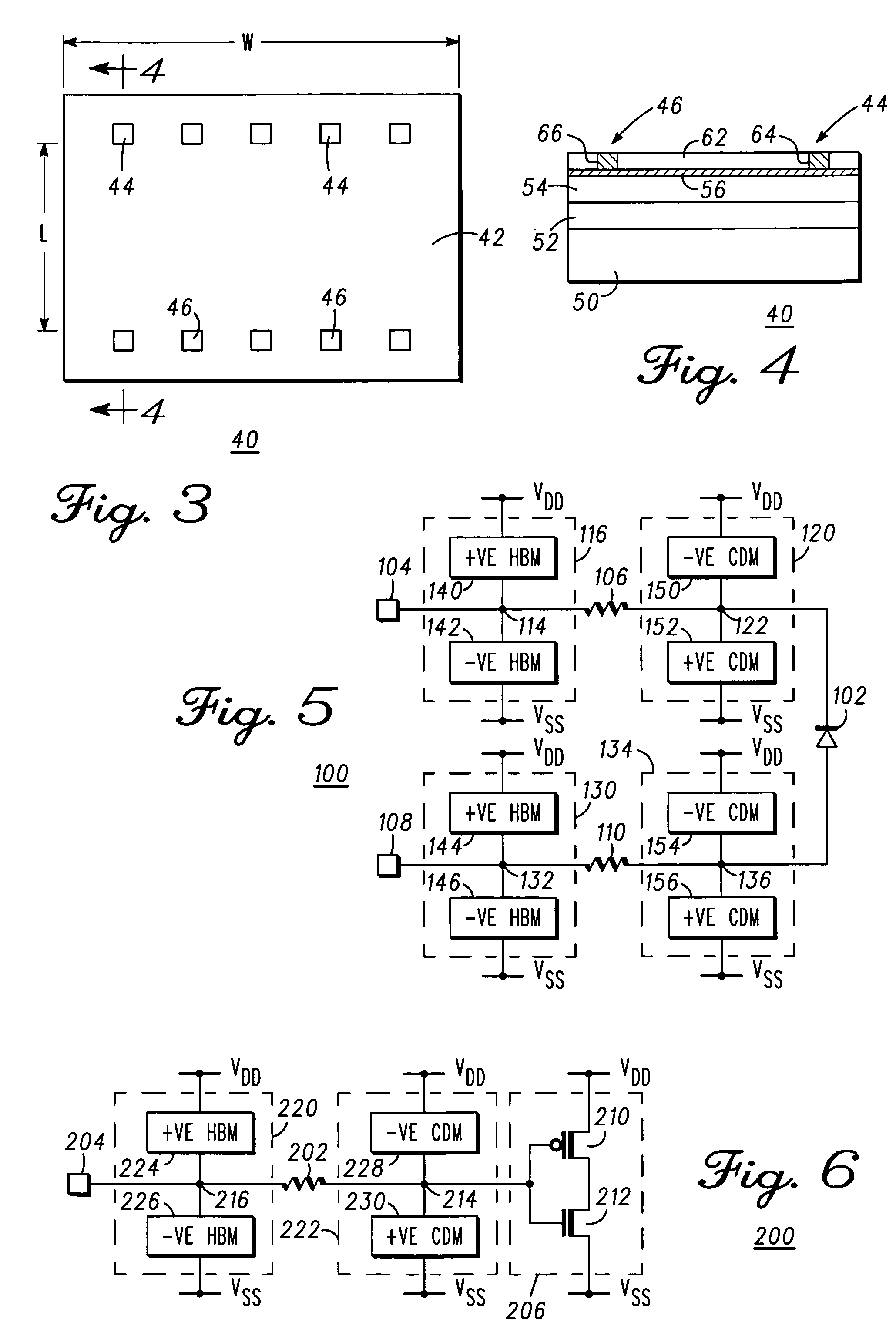
[0015]Generally, the present invention provides a semiconductor component having a tuned variable resistance resistor for protecting against a transient electrical signal such as, for example, an ESD event. The tuned variable resistance resistor has a low resistance value, e.g., 1 Ohm (Ω)–10Ω, in the absence of a large transient electrical signal and a high resistance value, e.g., 50Ω–200Ω in the presence of a large transient electrical signal. Semiconductor components having tuned variable resistance resistors are hardened to ESD events and are suitable for use in low frequency and high frequency applications. During normal operation, the resistance value is sufficiently low that high frequency performance is not degraded. During an ESD event, on the other hand, the resistance value of the tuned variable resistance resistor increases to prevent the device from becoming damaged. This protects the semiconductor component and ensures reliable operation should an ESD event occur.

[0016]...


PUM


Abstract

A semiconductor component having a tuned variable resistance resistor and a method for manufacturing the tuned variable resistance resistor. A semiconductor process for manufacturing a semiconductor component is selected. For the selected process, the tuned variable resistance resistor is characterized to determine the maximum stress current as a function of the width of the tuned variable resistance resistor. Then, for a given width and maximum stress current, the voltages across the resistors are characterized as a function of length. A tuned variable resistance resistor having a length and width capable of sustaining a predetermined maximum stress current is integrated into a semiconductor component. The semiconductor component may include protection circuitry designed in accordance with the Human Body Model, the Charge Device Model, or both.

Description

FIELD OF THE INVENTION[0001]This invention relates, in general, to semiconductor components and, more particularly, to the protection of semiconductor components from transient electrical signals.BACKGROUND OF THE INVENTION[0002]Semiconductor component manufacturers typically include structures for protecting their devices against failure caused by large transient electrical stimuli. When the stimulus is an electrostatic discharge (ESD) event, manufacturers generally incorporate protection structures that account for failure mechanisms attributed to the Human Body Model (HBM) and to the Charged Device Model (CDM). The Human Body Model simulates electrostatic discharge from a human body to a semiconductor device that is sensitive to the discharge event. Here, charge accumulated on the human body discharges to the semiconductor device. The Charged Device Model simulates the discharge of charge accumulated on the semiconductor device itself during the assembly process. When these charg...

Claims


Application Information

Patent Timeline
Patent Type & Authority Patents(United States)
IPC IPC(8): H01L29/00
CPCH01L28/20H01L27/0802
Inventor SALMAN, AKRAM A.BEEBE, STEPHEN G.
Owner GLOBALFOUNDRIES INC
Why Eureka
Try Eureka