Semiconductor carrier film, and semiconductor device and liquid crystal module using the same

a semiconductor and carrier film technology, applied in the direction of semiconductor devices, semiconductor/solid-state device details, instruments, etc., can solve the problem of weak current flowing in the barrier layer, and achieve the effect of higher output and a finer pitch

Active Publication Date: 2007-01-16
SHARP KK +1
View PDF3 Cites 34 Cited by
  • Summary
  • Abstract
  • Description
  • Claims
  • Application Information

AI Technical Summary

Benefits of technology

The present invention aims to provide a semiconductor carrier film that has better insulating resistance between terminals even in high temperature and moisture environments, allowing for a smaller distance between components and higher output. Additionally, the invention provides a semiconductor device and liquid crystal module that utilize this improved semiconductor carrier film.

Problems solved by technology

The technical problem addressed in this patent text relates to improving the insulating resistance between adjacent terminals when making a semiconductor carrier film using a metalizing process. A new issue arises where migration occurs between terminals with different potential differences caused by environmental factors like heat and humidity.

Method used


Image

  • Semiconductor carrier film, and semiconductor device and liquid crystal module using the same
  • Semiconductor carrier film, and semiconductor device and liquid crystal module using the same
  • Semiconductor carrier film, and semiconductor device and liquid crystal module using the same

Examples


examples 1 through 11

, COMPARATIVE EXAMPLES 1 AND 2

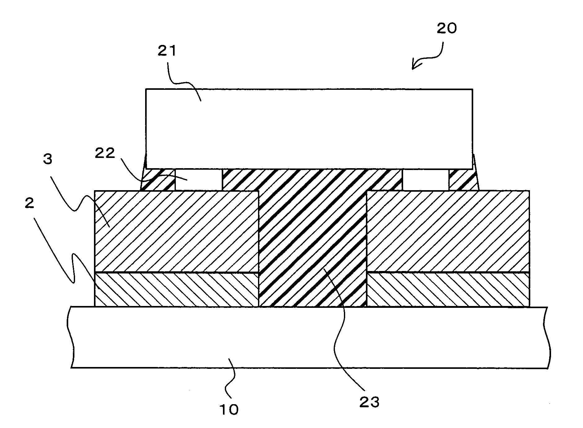
[0056]On a base film of polyimide having a thickness of 38 μm (product name: Esperflex; product of Sumitomo Metal Mining Co., Ltd.), a barrier layer 2 was formed by the spattering method. The barrier layer 2 included nickel-chrome alloy as a main component. Table 1 shows the ratio of chrome in the nickel-chrome alloy in Examples 1 through 11 and Comparative Examples 1 and 2. Table 1 also deals with other examples and comparative examples described later.

[0057]

TABLE 1PITCHRATIO OFTHICKNESS OFBETWEENCHROMEBARRIERTERMINALS% BY WEIGHTLAYER nmnmCOMPARATIVE77100EXAMPLE 1COMPARATIVE107100EXAMPLE 2EXAMPLE 1157100EXAMPLE 2207100EXAMPLE 3307100EXAMPLE 4507100EXAMPLE 52010100EXAMPLE 62015100EXAMPLE 72020100EXAMPLE 82025100EXAMPLE 92030100EXAMPLE 102035100EXAMPLE 112050100COMPARATIVE7740EXAMPLE 3EXAMPLE 12201540EXAMPLE 13203040COMPARATIVE1003540EXAMPLE 4COMPARATIVE7730EXAMPLE 5EXAMPLE 14201530COMPARATIVE1002030EXAMPLE 6

[0058]Next, on the barrier layer 2, a wire lay...

examples 12 and 13

, COMPARATIVE EXAMPLES 3 AND 4

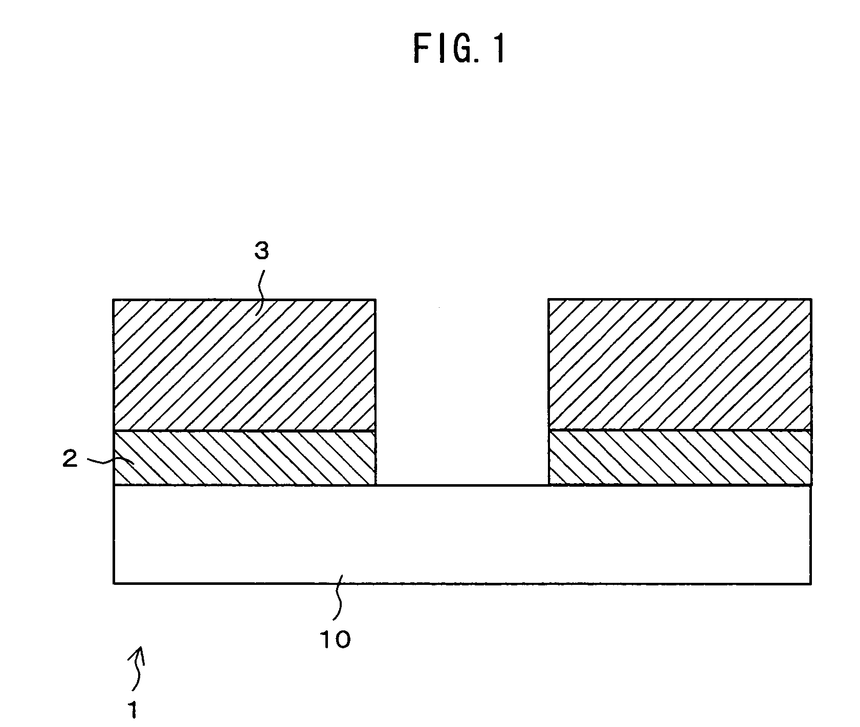
[0072]In the same manner as in Examples 1 through 11, the barrier layer 2 was formed on the base film, and the wire layer 3 was formed on the barrier layer 2. The barrier layer 2 was made of nickel-chrome alloy, and its ratio of chrome and thickness were as shown in Table 1 (see the sections of Examples 12 and 13, and Comparative Examples 3 and 4). The wire layer 3 was made of copper. Then, by the same method as in Example 2, etching was performed so as to form a comb-like wire pattern whose pitch between adjacent terminals was 40 μm (wire width: 20 μm, distance between adjacent terminals: 20 μm). In this way, the semiconductor carrier film 1 was produced. Onto a comb section, photoresist was applied in such a manner that a part of the comb section is exposed.

[0073]The semiconductor carrier film was put under the condition of normal temperature and moisture (20° C. and 25% RH), and a DC voltage (40V) was applied to adjacent terminals. Then, a leak curre...


PUM


Abstract

A semiconductor carrier film includes (i) a base film having insulating property, (ii) a barrier layer provided on the base film, the barrier layer including nickel-chrome alloy as a main component, and (iii) a wire layer provided on the barrier layer, the wire layer being made of conductive material including copper, and a ratio of chrome in the barrier layer is 15% to 50% by weight. A semiconductor device is formed by bonding a semiconductor element to the wire layer. The semiconductor carrier film and the semiconductor device are suitable for attaining finer pitches and higher outputs, because insulating resistance between adjacent terminals is less likely to deteriorate then in conventional art even in the environment of high temperature and moisture.

Description


Claims


Application Information

Patent Timeline
Owner SHARP KK
Why Eureka
Try Eureka