Sampling and level shifting circuit

a level shifting circuit and level shifting technology, applied in the field of circuits, can solve the problems of significantly increasing the area of circuitry and significantly affecting the cost of an integrated circuit, and achieve the effect of linearizing the charge transfer

Inactive Publication Date: 2007-01-23
ATMEL CORP
View PDF5 Cites 10 Cited by
  • Summary
  • Abstract
  • Description
  • Claims
  • Application Information

AI Technical Summary

Problems solved by technology

This large capacitance can significantly affect the cost of an integrated circuit as well as significantly add to the area of the circuitry.

Method used


Image

  • Sampling and level shifting circuit
  • Sampling and level shifting circuit
  • Sampling and level shifting circuit

Examples


Embodiment Construction

[0008]The present invention relates generally to circuitry and more specifically to sampling and level shifting circuitry. The following description is presented to enable one of ordinary skill in the art to make and use the invention and is provided in the context of a patent application and its requirements. Various modifications to the preferred embodiments and the generic principles and features described herein will be readily apparent to those skilled in the art. Thus, the present invention is not intended to be limited to the embodiments shown, but is to be accorded the widest scope consistent with the principles and features described herein.

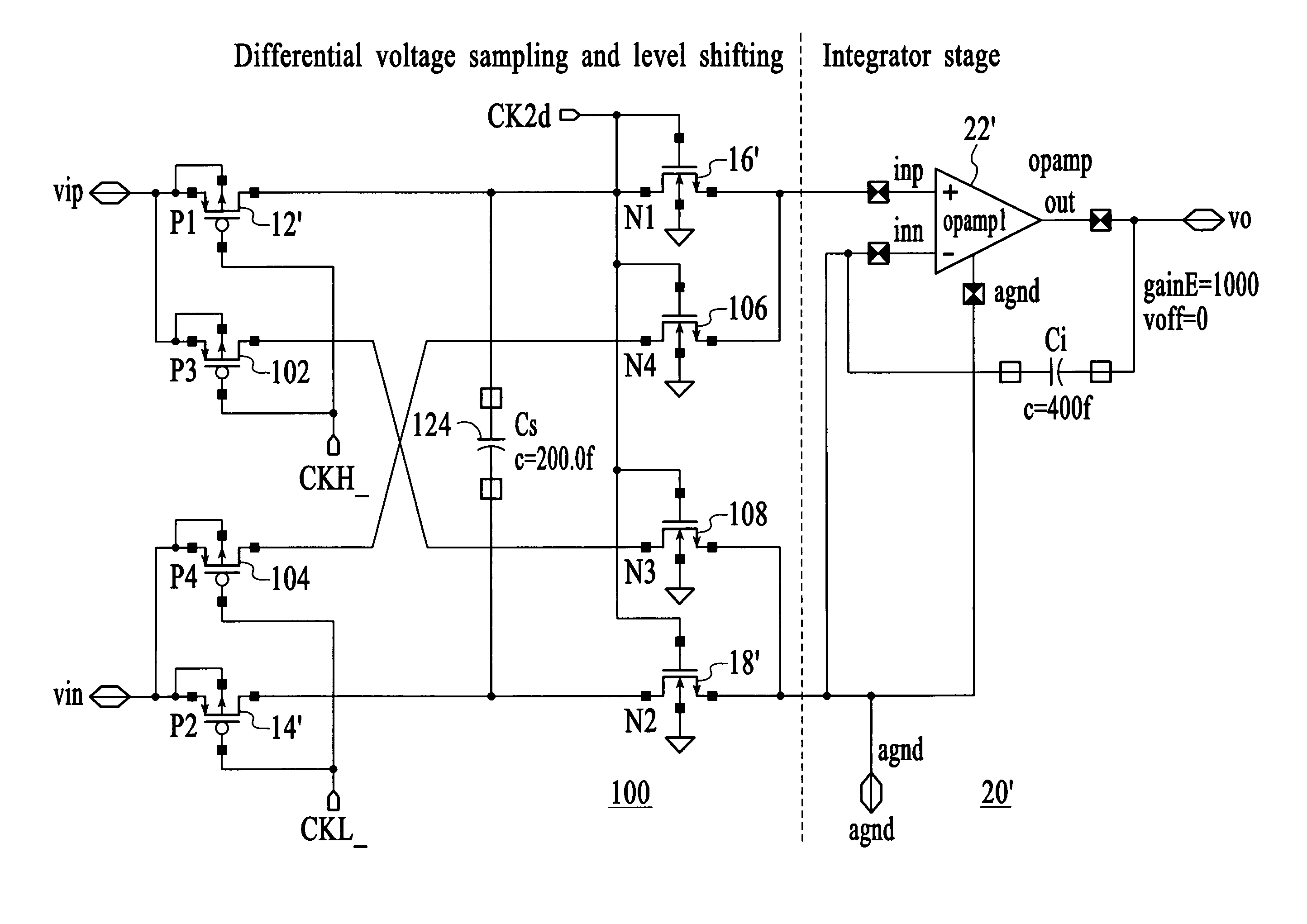
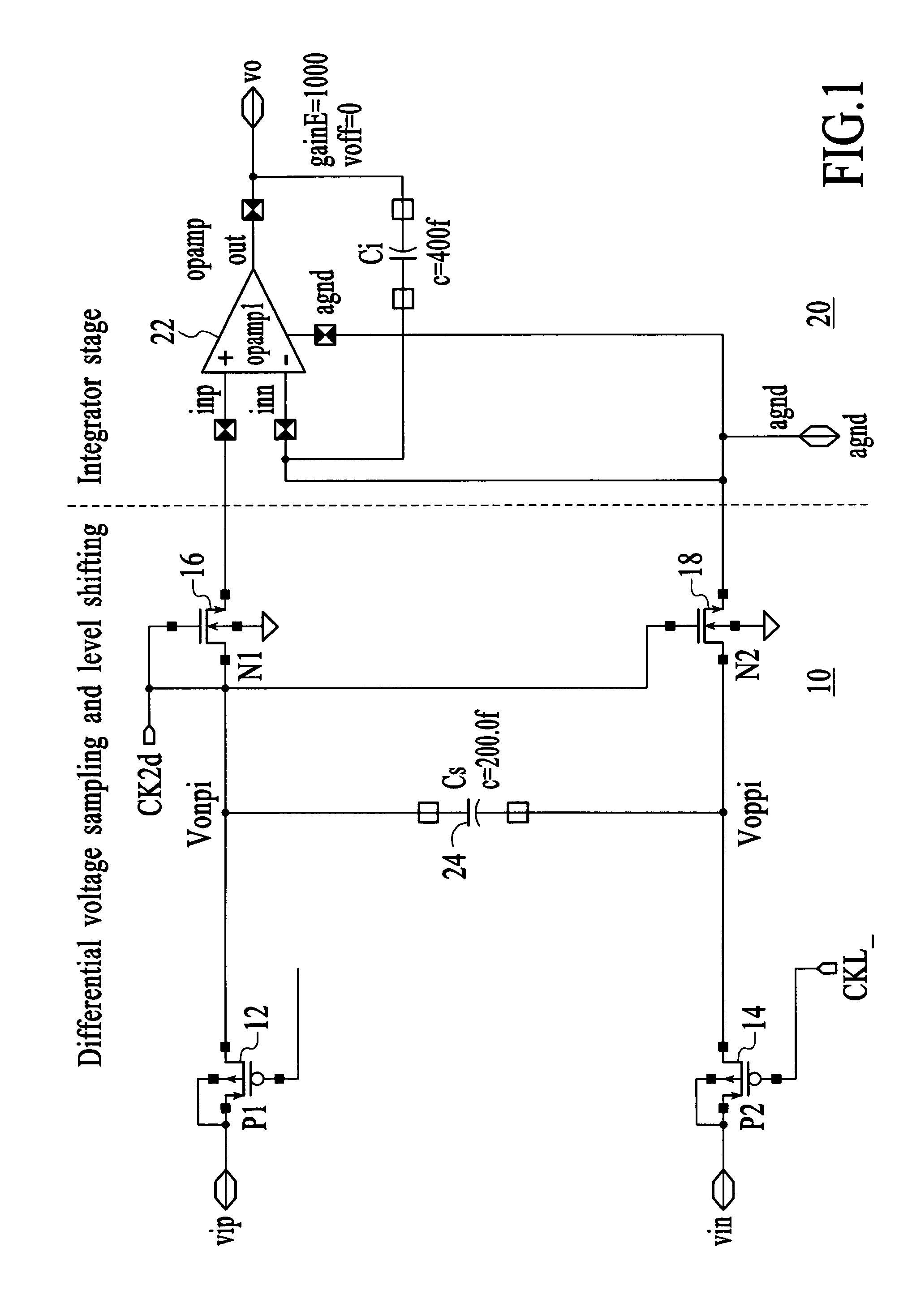
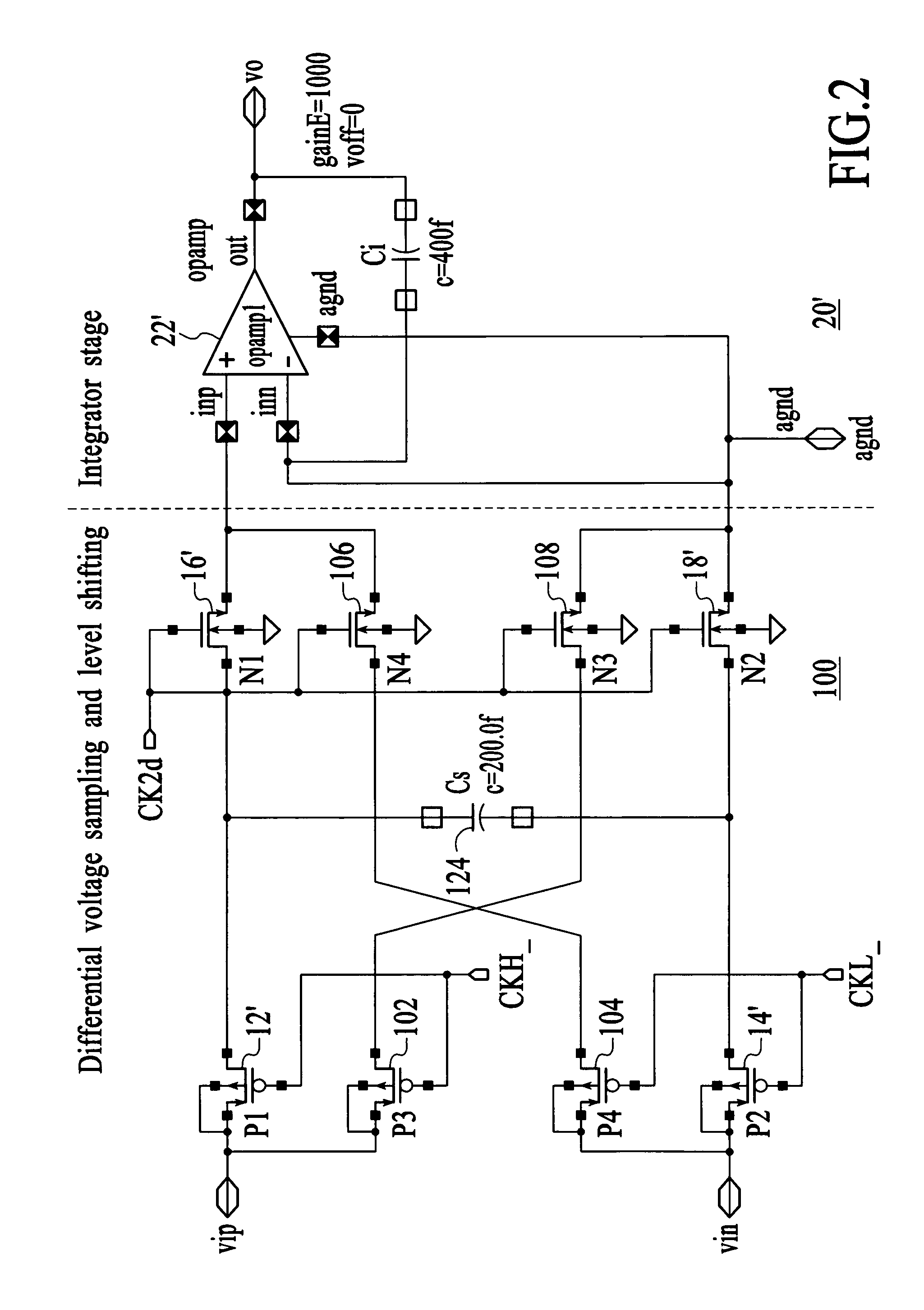
[0009]Circuitry to cancel the effect of parasitic non-linear capacitances when sampling and level-shifting differential voltages is disclosed. FIG. 1 is a diagram of a conventional sampling and level shifting circuit 10. The sampling level shifting circuit 10 comprises a first PMOS transistor 12 which receives a first voltage Vip (for ex...


PUM


Abstract

A circuit comprising a first switch for sampling a differential signal and a second switch for level-shifting the sampled differential signal is disclosed. The first and second switches are cross-coupled to cancel a charge injected between the first and second switches and for linearizing the charge transfer; and a capacitor coupled is between the first and second switches. A circuit in accordance with the present invention adds an extra sampling switch to the sampling circuit and an extra charge-transfer switch in the level-shifting circuit. By cross-coupling these extra switches, the result is a cancellation of the charge-injection, and thus linearizing the charge transfer.

Description

FIELD OF THE INVENTION[0001]The present invention relates generally to circuitry and more specifically to sampling and level shifting circuitry.BACKGROUND OF THE INVENTION[0002]In many types of circuits it is desirable to cancel the effects of parasitic nonlinear capacitances when sampling and level shifting differential voltages. Examples of such circuits are analog to digital converters (ADCs) and digital signal processors. In a circuit which has a 2.5 differential voltage, a sampling capacitor of 20 picoFarads is employed to suppress the effect of the non-linear capacitances. This large capacitance can significantly affect the cost of an integrated circuit as well as significantly add to the area of the circuitry.[0003]Accordingly, what is needed is a system and method for providing sampling and level shifting circuitry which does not require large capacitances and therefore is less costly and utilizes less area in an integrated circuit. The circuitry, system and method should be...

Claims


Application Information

Patent Timeline
Patent Type & Authority Patents(United States)
IPC IPC(8): G11C27/02H03K5/00
CPCG11C27/026
Inventor SOERAASEN, RUNAR
Owner ATMEL CORP
Why Eureka
Try Eureka