Photomask features with interior nonprinting window using alternating phase shifting

a technology of alternating phase shifting and photomasks, which is applied in the direction of photomechanical devices, relative volume flow measurements, instruments, etc., can solve the problems of reducing the resolution of the image, reducing the accuracy of the image,

Active Publication Date: 2007-02-06
SANDISK TECH LLC
View PDF8 Cites 118 Cited by
  • Summary
  • Abstract
  • Description
  • Claims
  • Application Information

AI Technical Summary

Problems solved by technology

As projected features become smaller, the limits of resolution are reached and it becomes more difficult to project patterns with sharp edges.
Poor resolution can lead to incomplete patterning and to incomplete etching or overetching, causing device flaws.
The use of alternating phase shifters in photomasks, however, has disadvantages.
The configuration of some patterns leads to phase conflicts, in which rules dictate that the same area must see light of opposite phases.
To date, this has meant that use of alternating phase shifters has been limited to only certain types of patterns.
Alternating phase shifters also typically require use of a trim mask, adding extra cost and processing time.

Method used


Image

  • Photomask features with interior nonprinting window using alternating phase shifting
  • Photomask features with interior nonprinting window using alternating phase shifting
  • Photomask features with interior nonprinting window using alternating phase shifting

Examples


Embodiment Construction

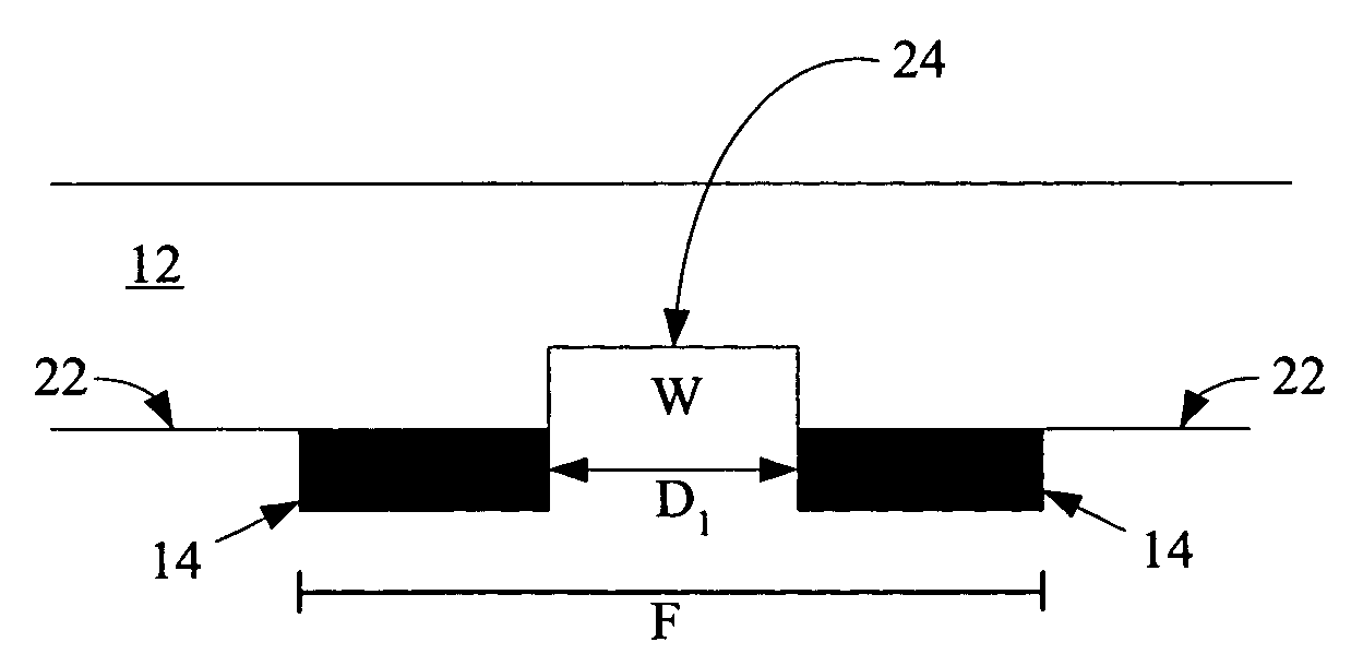
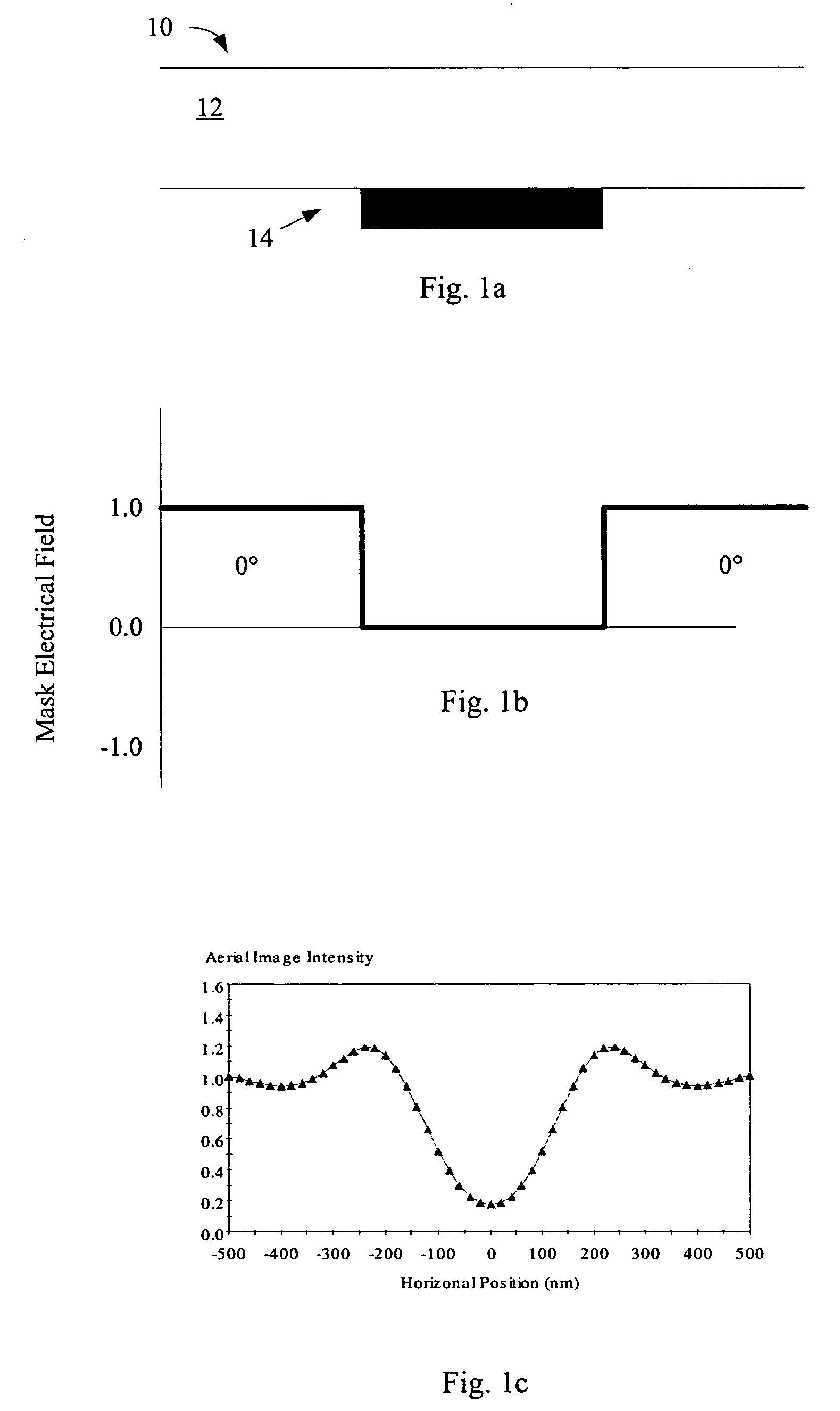
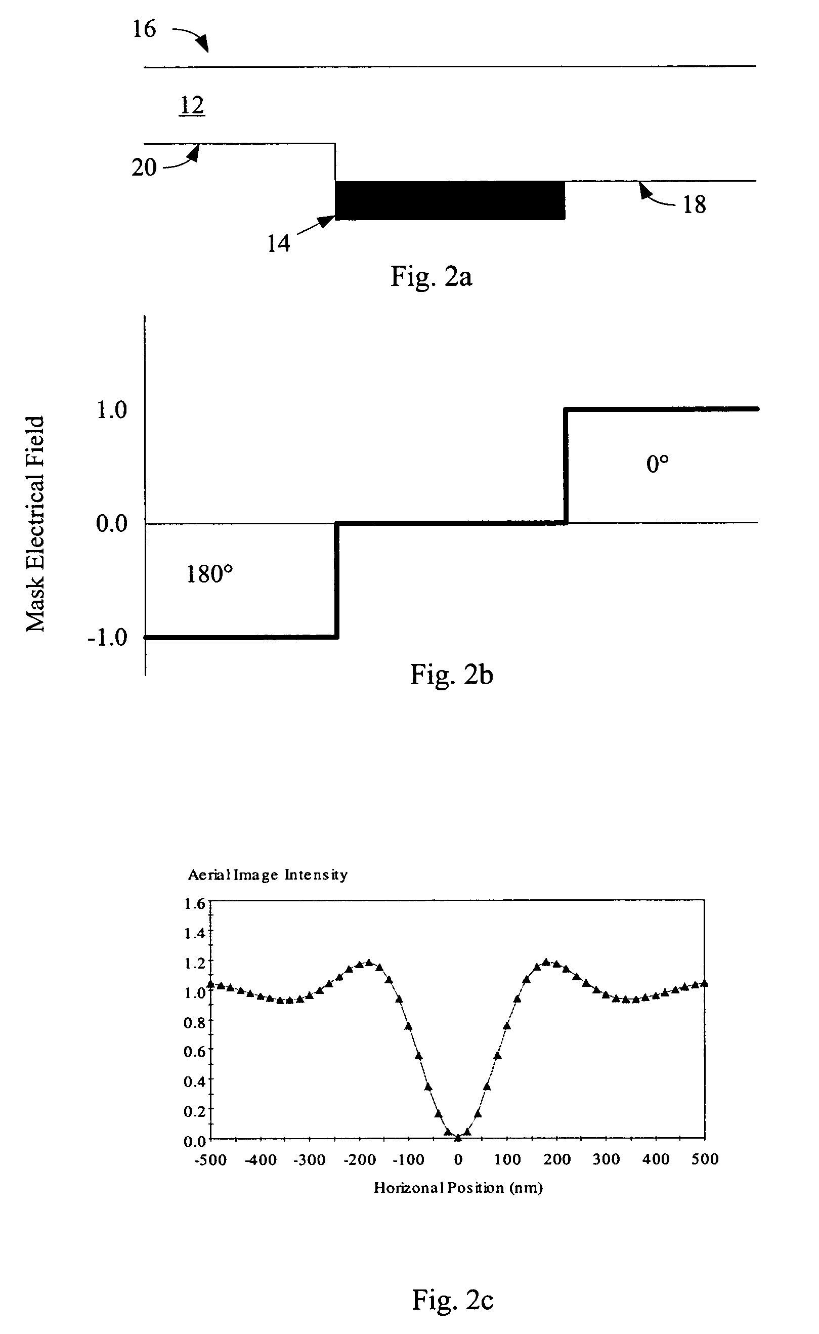
[0037]As described earlier, as part of the process of forming patterned features on an integrated circuit, light is projected through a photomask onto a photoresist surface. A feature in a mask is projected onto photoresist, then the photoresist feature is used to etch a feature in an underlying material, or in multiple layers of materials.

[0038]In this description, a masked feature will refer to a feature in a photomask. Such a feature may be a line, a rectangle, or any other shape. A masked feature in a photomask substantially entirely or partially obscures light, so that when light is projected through the photomask, a corresponding feature in the photoresist is shielded from light, while the area outside of the obscured area is exposed. This corresponding feature in photoresist will be called a projected photoresist feature. The projected photoresist feature will be roughly the same shape as the masked feature, though corners on projected photoresist features tend to be rounded....


PUM

PropertyMeasurementUnit
wavelengthaaaaaaaaaa

Abstract

Aspects of the present invention provide for a novel photomask for patterning features for an integrated circuit, the photomask including masked features having interior nonprinting windows. In some embodiments, the interior nonprinting window is an alternating phase shifter, while the area surrounding the masked features transmits light unshifted. In other embodiments, the interior nonprinting window transmits light unshifted, while the area surrounding the masked features is an alternating phase shifter. Thus any arrangement of features can be patterned with no phase conflict.

Description

BACKGROUND OF THE INVENTION[0001]The invention relates to a method for patterning fine features for semiconductor devices using an alternating phase shifting mask.[0002]Patterned features making up integrated circuits are conventionally formed using photolithography and etch techniques. A photomask, which transmits light in some areas and blocks it in others, is formed, the blocking areas corresponding to the pattern to be formed on the wafer surface (or its inverse.) The surface to be patterned, for example a semiconductor or dielectric layer, is covered with a layer of photoresist, a photoreactive material. Light is projected onto the photoresist surface using the photomask, selectively exposing areas of photoresist. The wafer is then subjected to a developing process, in which exposed photoresist (or unexposed photoresist, in the case of negative photoresist) is removed, leaving patterned photoresist behind.[0003]The remaining patterned photoresist then typically serves to protec...

Claims


Application Information

Patent Timeline
Patent Type & Authority Patents(United States)
IPC IPC(8): G01F9/00G03C5/00G03F1/00G03F9/00
CPCG03F1/30
Inventor CHEN, YUNG-TIN
Owner SANDISK TECH LLC
Why Eureka
Try Eureka