Method and circuit for translating a differential signal to complementary CMOS levels

a technology of differential signal and complementary cmos, applied in logic circuits, logic circuit coupling/interface arrangements, pulse techniques, etc., can solve the problems of not being able to accept some implementations, rising time to become faster than fail time, etc., and achieve accurate translation.

Active Publication Date: 2007-02-06
MONTEREY RES LLC
View PDF2 Cites 15 Cited by
  • Summary
  • Abstract
  • Description
  • Claims
  • Application Information

AI Technical Summary

Benefits of technology

[0013]Some embodiments of the invention provide a method for accurately translating a differential signal into a complementary CMOS signal. Other embodiments of the invention provide a circuit for accurately translating a differential signal into a complementary CMOS signal.

Problems solved by technology

Also, the trip point of the first inverter INV1 is generally skewed upwards, which causes the rise time to become faster than the fail time.
For example, a 1.2 ns input width may be reduced to 1.0 ns at the output, which may not be acceptable for some implementations.

Method used


Image

  • Method and circuit for translating a differential signal to complementary CMOS levels
  • Method and circuit for translating a differential signal to complementary CMOS levels
  • Method and circuit for translating a differential signal to complementary CMOS levels

Examples


Embodiment Construction

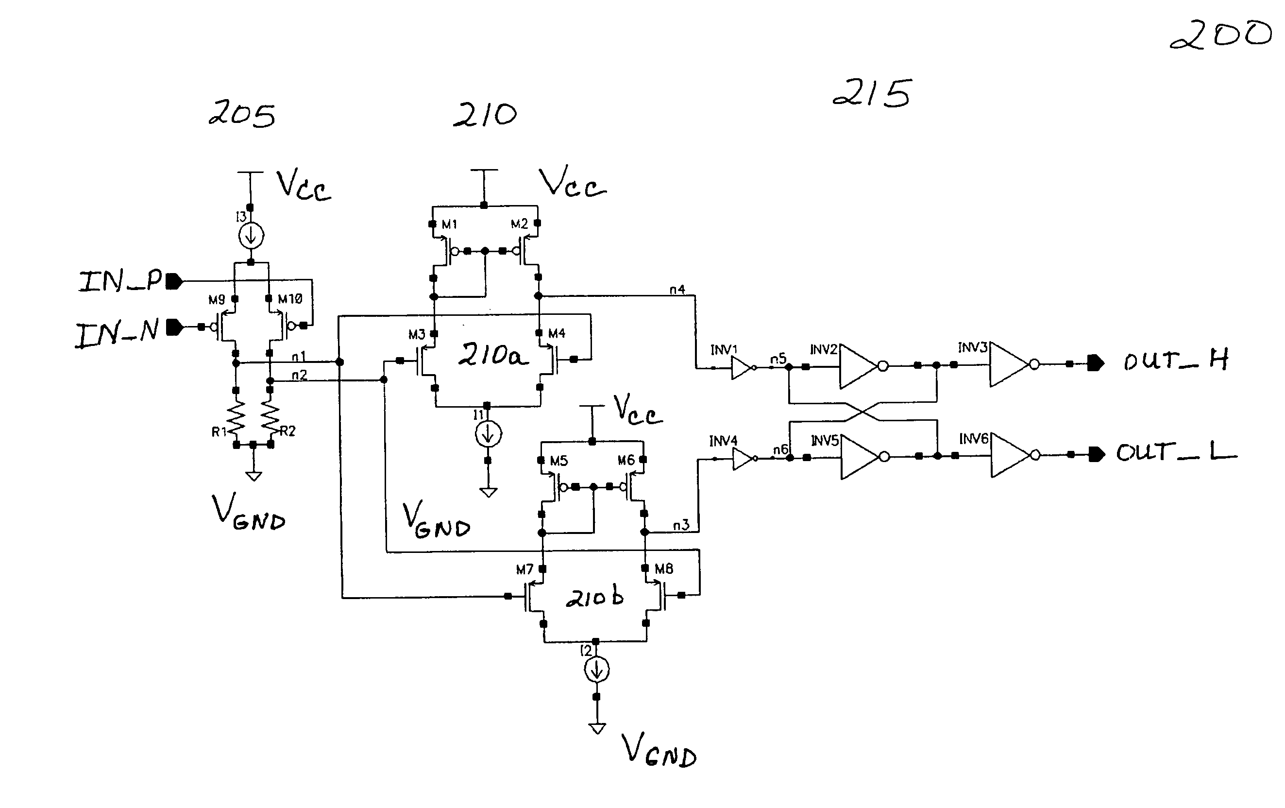
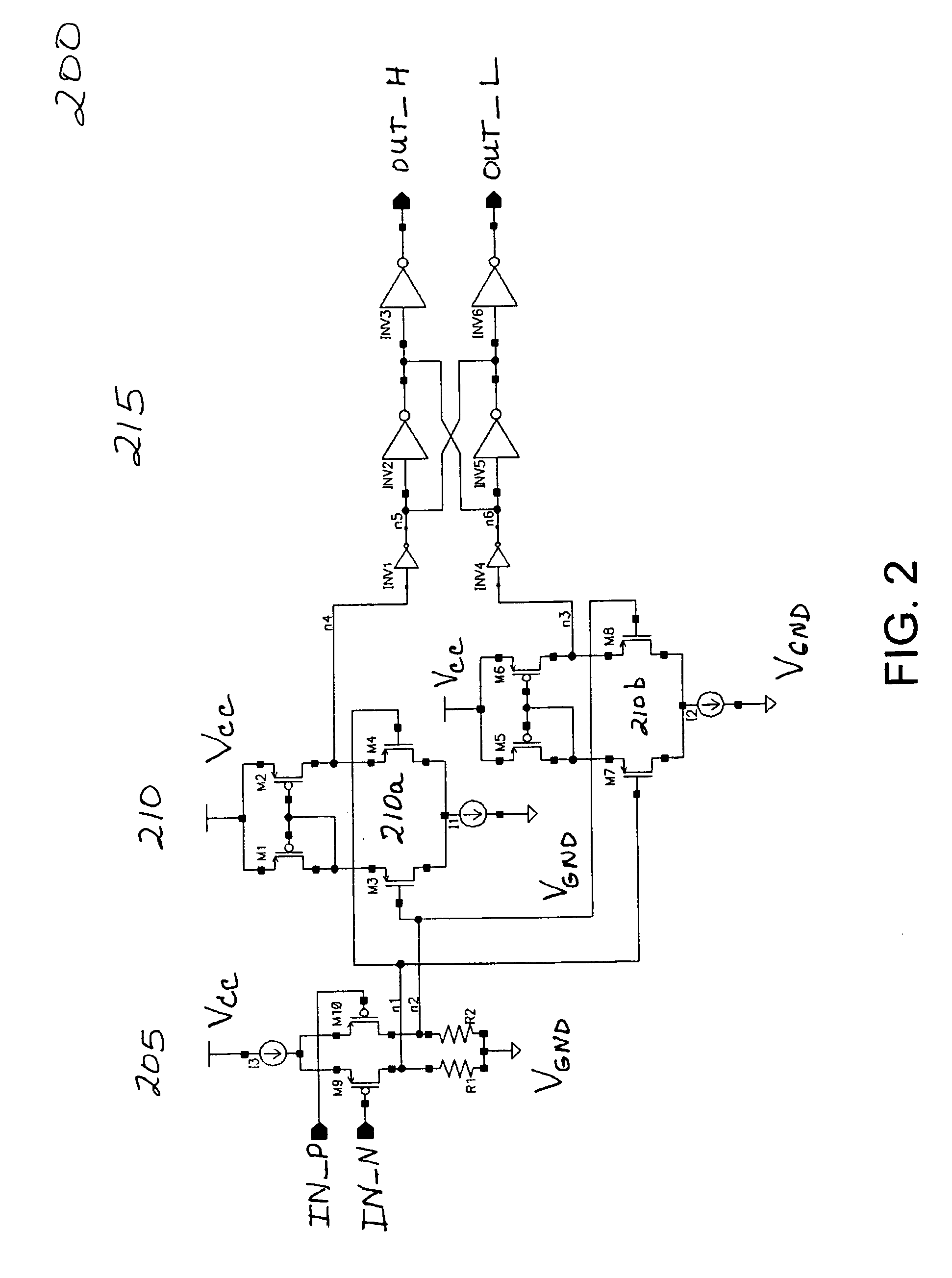
[0018]FIG. 2 is a circuit diagram illustrating an improved level translator circuit 200 according to some embodiments of the invention. The improved level translator circuit 200 includes a buffer section 205, a differential to single ended section 210, and a delay equalizing latch section 215.

[0019]The buffer section includes a current source 13, two PMOS transistors M9 and M10, and two resistors R1 and R2. Each of the transistors M9, M10 is serially connected with one of the resistors R1, R2. It is preferable that the transistors M9, M10 be relatively well-matched devices in order to effectively eliminate common mode noise. Similarly, it is desirable that the resistors R1, R2 have approximately the same resistance.

[0020]Each series combination of transistor / resistor is connected in parallel between the current source 13 and the ground node VGND. The circuit nodes n1, n2 are used to drive the differential to single ended stage 210. Differential inputs IN_P, IN_N are applied to the g...


PUM


Abstract

A circuit according to some embodiments of the invention includes a first differential to single ended translator having a first output, a second differential to single ended translator having a second output, and a latch coupled to the first output and the second output, where the latch is configured to select the slower of the first output and the second output.

Description

CROSS REFERENCE TO RELATED APPLICATIONS[0001]This application claims priority from U.S. provisional patent application Ser. No. 60 / 531,527 filed on 18 Dec. 2003, entitled Method and Circuit for Translating a Differential Signal to Complementary CMOS Levels, which is hereby incorporated by reference in its entirety for all purposes.BACKGROUND OF THE INVENTION[0002]1. Technical Field of the Invention[0003]This disclosure relates generally to electronic circuits, and in particular to circuits for level translation.[0004]2. Description of the Related Art[0005]Level translation moves a signal from a first signaling voltage swing domain to a second domain. This translation is usually from a low-swing domain to a high-swing domain.[0006]A common conventional solution for translating differential signals (usually at a lower voltage level) to complementary metal oxide silicon (CMOS) signals (usually at a higher voltage level) is to use a differential amplifier with a single ended output driv...

Claims


Application Information

Patent Timeline
Patent Type & Authority Patents(United States)
IPC IPC(8): H03K19/0175H03K19/0185
CPCH03K19/018528
Inventor PRATHER, STEPHEN M.BERZINS, MATTHEW S.WALDRIP, JEFFREY W.
Owner MONTEREY RES LLC
Why Eureka
Try Eureka