Method of fabricating copper damascene and dual damascene interconnect wiring

a technology of damascene and interconnect wires, which is applied in the direction of semiconductor/solid-state device manufacturing, basic electric elements, electric devices, etc., can solve the problems of aluminum having problems associated with heat dissipation and electro-migration, fabricating copper interconnects

Inactive Publication Date: 2007-02-13
AURIGA INNOVATIONS INC
View PDF9 Cites 13 Cited by
  • Summary
  • Abstract
  • Description
  • Claims
  • Application Information

AI Technical Summary

Benefits of technology

[0005]A third aspect of the present invention is an integrated circuit, comprising: a copper damascene or dual damascene wire in a fluorinated silicon glass dielectric layer, a top surface of the copper damascene or dual damascene wire coplanar with a top surface of the fluorinated silicon glass dielectric layer; a first capping layer formed on the top surface of the copper damascene or dual damascene wire and the top surface of the fluorinated silicon glass dielectric layer; and a second capping layer formed on the top surface of the first capping layer, the first capping layer thin enough to allow performance of one or more characterization procedures in relation to the integrated circuit and thick enough to prevent formation, on the top surface of the copper damascene or dual damascene wire, of copper containing particles by reaction of copper in the copper damascene or dual damascene wire with fluorine in the fluorinated silicon glass dielectric layer.

Problems solved by technology

For example, aluminum has problems associated with heat dissipation and electro-migration.
However, there are difficulties with fabricating copper interconnects because copper is more reactive than aluminum and can diffuse through many dielectric materials complicating the fabrication process of copper wiring.

Method used


Image

  • Method of fabricating copper damascene and dual damascene interconnect wiring
  • Method of fabricating copper damascene and dual damascene interconnect wiring
  • Method of fabricating copper damascene and dual damascene interconnect wiring

Examples


first embodiment

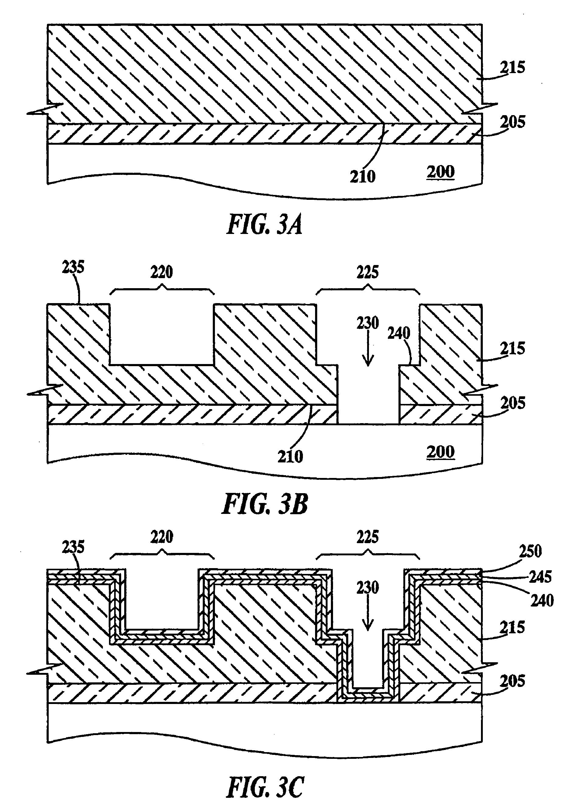
[0024]FIGS. 3A through 3I are partial cross-sectional views of a method of fabricating copper interconnect wires according to the present invention. FIGS. 3A through 3I illustrate the present invention using a dual damascene process. The invention is equally applicable to single damascene processing where vias and studs are formed in adjacent levels to the wiring levels.

[0025]In FIG. 3A, formed on a substrate 200 is a dielectric copper diffusion barrier 205 and formed on a top surface 210 of dielectric copper diffusion barrier 205 is an ILD layer 215. In one example dielectric copper diffusion barrier layer 205 comprises SixNy and is about 350 Å to about 900 Å thick. In one example, ILD layer 215 is FSG containing about 1% to about 9% fluorine by weight and is about 0.2 microns to about 6 microns thick. Formation of SixNy by plasma-enhanced chemical-vapor-deposition (PECVD) is well known in the art. In a first example, FSG may be formed in a PECVD or high-density plasma CVD (HDPCVD)...

second embodiment

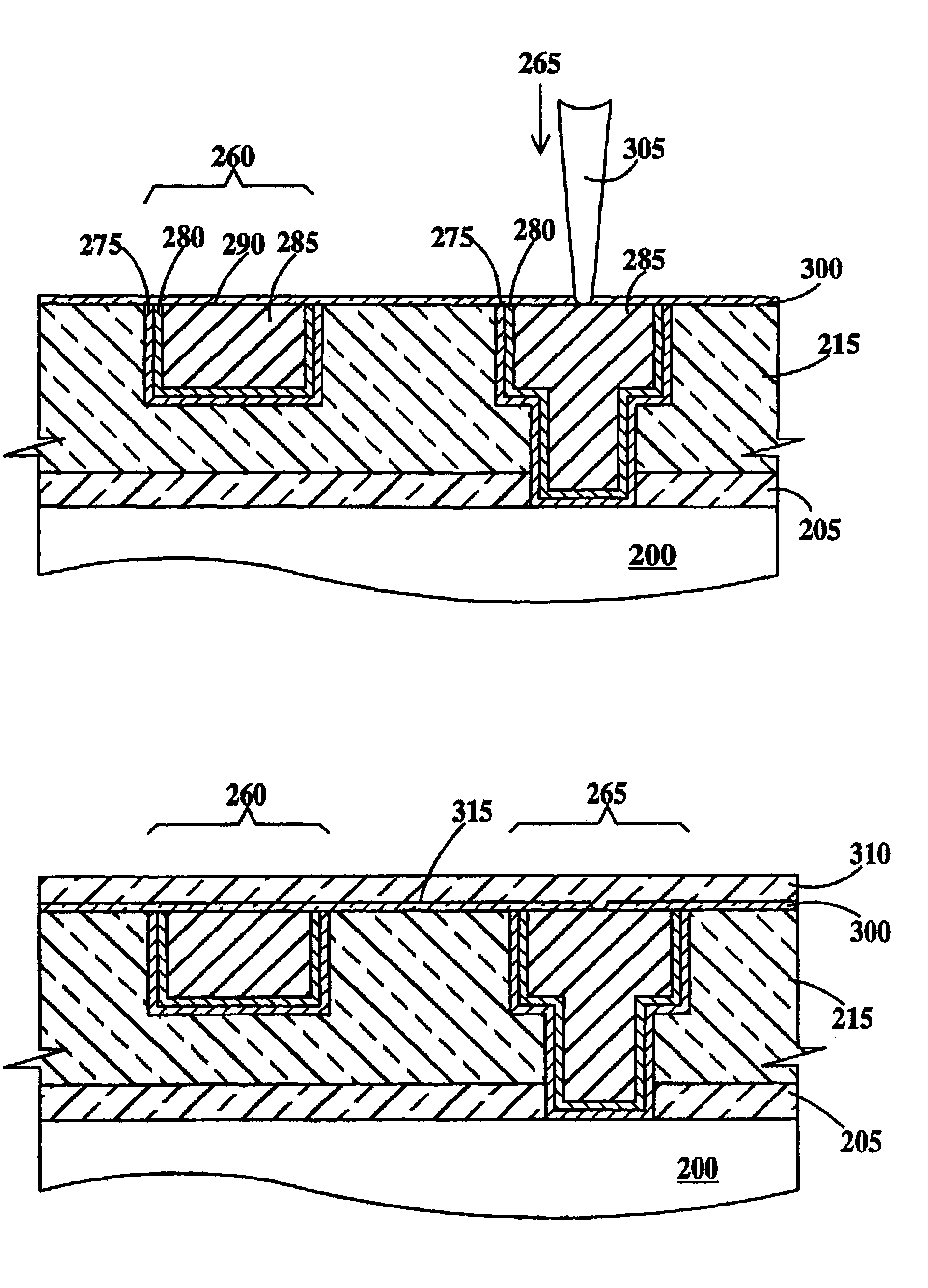
[0035]FIGS. 4A and 4B are partial cross-sectional views of a method of fabricating copper interconnect wires according to the present invention. In FIG. 4A, first capping layer 300A comprises a lower first capping layer 330 and an upper first capping layer 335. In one example, lower first capping layer 330 and upper first capping layer 335 each independently comprise SixNy, SixCy, SiCxHy, SiCxOyNz or SiCxNy. In one example, lower first capping layer 330 and upper first capping layer 335 are independently about 25 Å to about 100 Å thick. All capping layers of the present invention may comprise multiple layers as discussed infra.

[0036]In a first example, the total thickness (the thickness of lower first capping layer 330 plus the thickness of upper first capping layer 335) of first capping layer 300A is selected to be thin enough to allow optical microscopy and scanning electron microscopy (SEM) defect inspection and image size measurements of dual structures under the capping layer. ...

third embodiment

[0038]In the present invention first capping layer 300 and second capping layer 310 each independently comprise two or more layers of materials selected from the group consisting of SixNy, SixCy, SiCxHy, SiCxOyNz and SiCxNy, each layer of first capping layer 300 being, for example, between about 25 Å to about 100 Å thick and each layer of second capping layer 305 being, for example, between about 150 Å to about 700 Å thick.

[0039]FIG. 5 is a flowchart of the method of fabricating copper interconnect wires according to the present invention. The method may be practiced as described supra or may incorporate controlled storage and rework cleans as described infra.

[0040]In step 400, a substrate is provided with an ILD layer over a copper diffusion barrier layer as describe supra in reference to FIG. 3A. In one example, the substrate is a 200 mm or 300 mm bulk silicon or silicon-on insulator (SOI) semiconductor wafer. In step 405, wire trenches (and optionally via opening in the bottom of...


PUM

PropertyMeasurementUnit
temperatureaaaaaaaaaa
thickaaaaaaaaaa
thicknessaaaaaaaaaa

Abstract

An integrated circuit and a method of manufacturing the integrated circuit, the method including: (a) providing a substrate; (b) forming a copper diffusion barrier layer on the substrate; (c) forming a dielectric layer on a top surface of the copper diffusion barrier layer; (d) forming a copper damascene or dual damascene wire in the dielectric layer, a top surface of the copper damascene or dual damascene wire coplanar with a top surface of the dielectric layer; (e) forming a first capping layer on the top surface of the wire and the top surface of the dielectric layer; (f) after step (e) performing one or more characterization procedures in relation to said integrated circuit; and (g) after step (e) forming a second capping layer on a top surface of the first capping layer.

Description

FIELD OF THE INVENTION[0001]The present invention relates to the field of integrated circuit fabrication; more specifically, it relates to method of fabricating copper damascene and dual damascene wires.BACKGROUND OF THE INVENTION[0002]Semiconductor manufacturers must contend with continually decreasing device sizes, wire widths and wire thicknesses and power consumption as well as increasing device density, wire density and operating frequencies. These requirements have led the semiconductor industry to utilize copper wiring in place of older wire materials, for example, those based on aluminum and aluminum alloys. For example, aluminum has problems associated with heat dissipation and electro-migration. Copper, which has a lower resistivity and greater electro-migration lifetime eliminates many of the problems associated with aluminum and is more suitable for use in low-power, low-voltage and high speed applications. However, there are difficulties with fabricating copper intercon...

Claims


Application Information

Patent Timeline
Patent Type & Authority Patents(United States)
IPC IPC(8): H01L21/4763
CPCH01L21/76802H01L21/76834H01L21/76832H01L21/76807
Inventor GAMBINO, JEFFREY P.HILL, WILLIAMMCAVEY, JR., KENNETH F.MCDEVITT, THOMAS L.STAMPER, ANTHONY K.WINSLOW, ARTHUR C.ZWONIK, ROBERT
Owner AURIGA INNOVATIONS INC
Why Eureka
Try Eureka