Selective formation of metallic films on metallic surfaces

Active Publication Date: 2013-08-01
ASM INTERNATIONAL
View PDF2 Cites 310 Cited by
  • Summary
  • Abstract
  • Description
  • Claims
  • Application Information

AI Technical Summary

Benefits of technology

[0014]In some embodiments, selective deposition comprises alternately exposing the substrate to a first reactant and a second reactant, where the second reactant is different from the first reactant. The methods may also comprise a dielectric surface restoration step. For example, the dielectric surface may be

Problems solved by technology
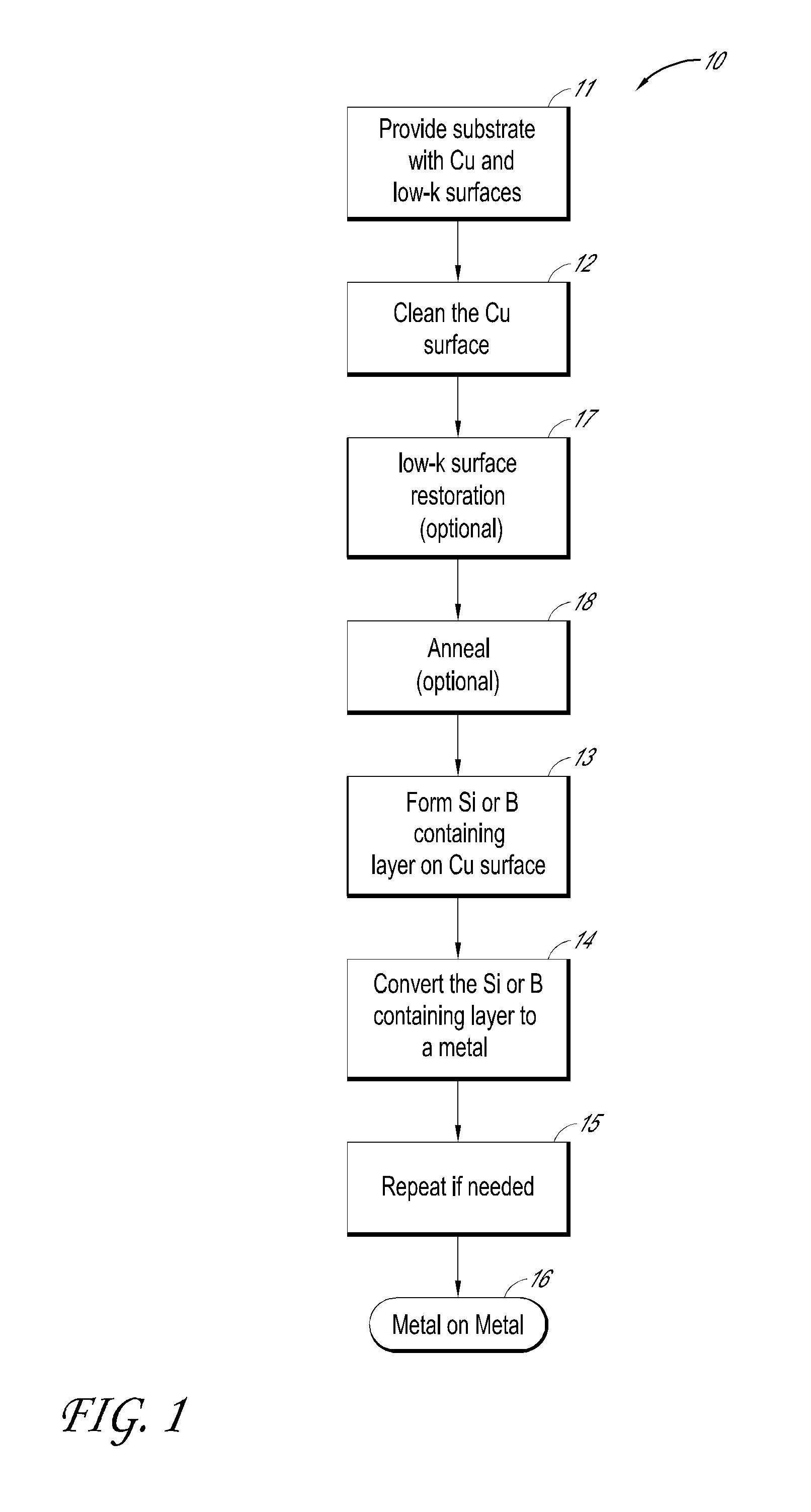
Meeting the ever increasing electromigration (EM) requirement in copper interconnects is becoming more difficult as Moore's law progresses, resulting in smaller devices.
As line dimensions shrink, critical void size for EM failur

Method used


Image

  • Selective formation of metallic films on metallic surfaces
  • Selective formation of metallic films on metallic surfaces
  • Selective formation of metallic films on metallic surfaces

Examples


example 1

[0124]To selectively deposit a metallic layer on a metal surface, for example, the surface is preferably very clean. The cleaning may be conducted via gas or liquid phase. Specifically for copper, citric acid or some other later-generation cleaning agents may be used in the liquid phase to remove the commonly employed benzotriazole (BTA) passivating agent from the surface. Alternatively, NH3 or N2 / H2 containing plasma may be used as a gas phase approach to remove the BTA layer. Finally, H-radicals are used to ensure the surface is void of any oxidized copper.

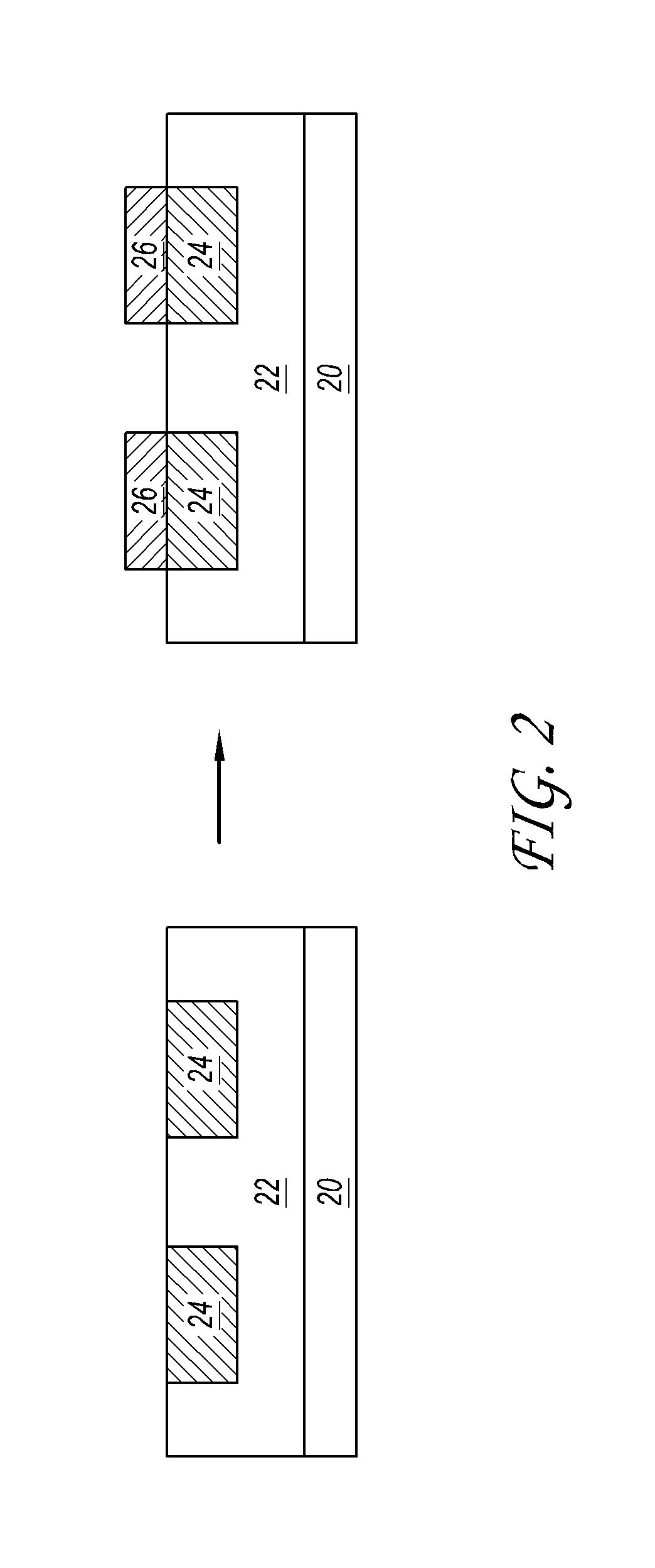
[0125]FIGS. 2 and 3 show schematic representations in accordance with some embodiments. FIG. 2 illustrates a substrate 20 with a silicon dioxide 22 insulating region and a copper surface 24. Selective deposition (not shown) is performed to deposit metal 26 on the copper regions 24 of the substrate while avoiding deposition on the SiO2 22.

[0126]FIG. 3 shows a schematic representation of a selective deposition process using disila...

example 2

[0128]A copper piece was cut and cleaned with citric acid. The citric acid solution was prepared by mixing approximately 5 g of citric acid crystals in 50 ml of water. The solution was stirred until all crystals had dissolved. A fresh solution was prepared for each film deposition run and discarded immediately after use. The copper piece was dipped in the solution, left immersed for 30 seconds, and stirred a few times during that period. The copper piece was then lifted and dried by draining the liquid back into the solution. If the piece was dried by nitrogen blowing, water marks were produced. Finally, the back side of the copper piece was dried by placing the piece on a piece of clean room tissue. The cleaned copper piece was then placed onto an adapter wafer and loaded into a vacuum load lock within three minutes of cleaning.

[0129]After loading the copper piece into the vacuum load lock, it was transported by vacuum transport into the reaction chamber. The film deposition took p...

example 3

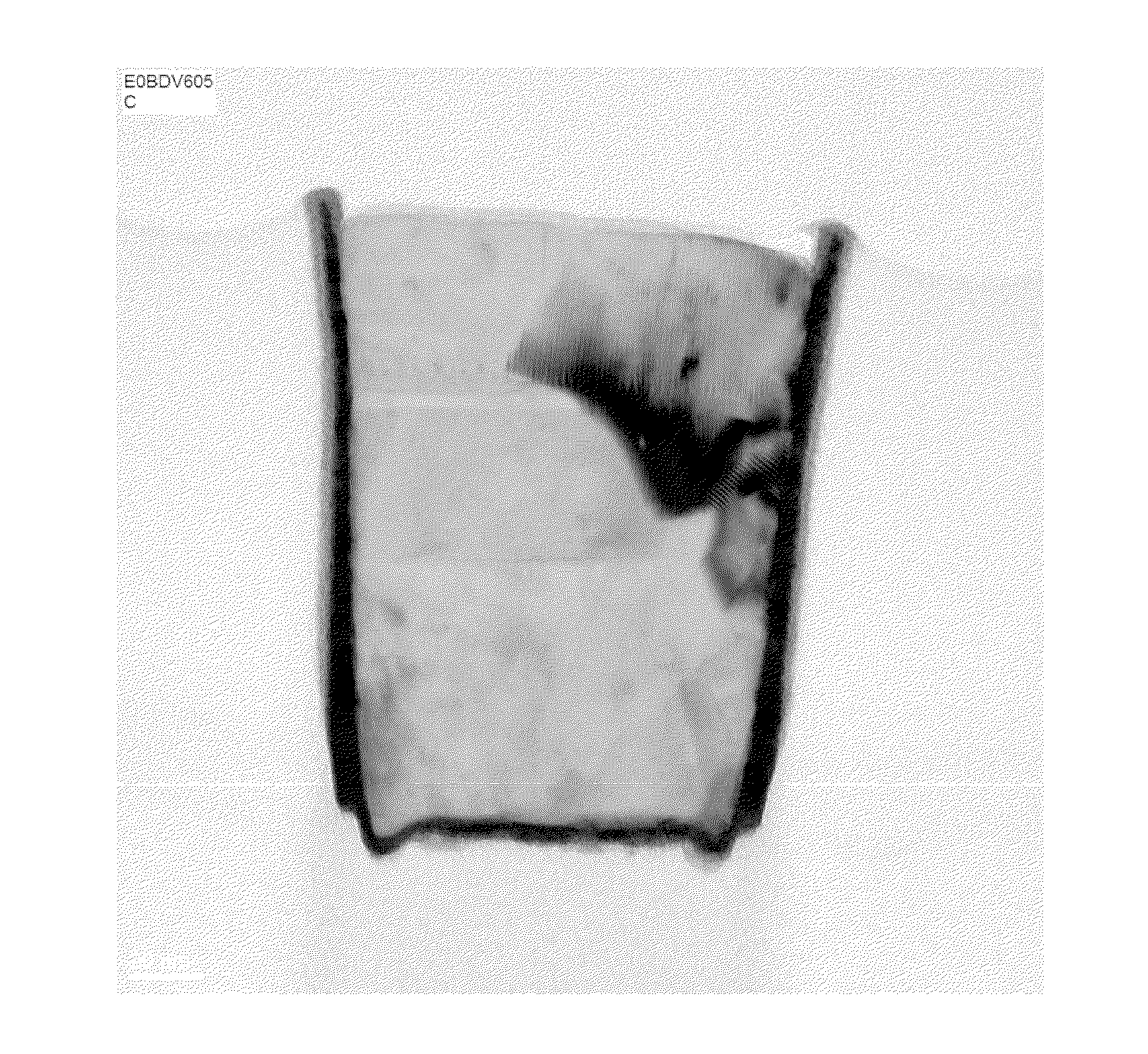
[0134]A sample comprising copper lines embedded in a low-k material (ELK 2.3) was provided. Tungsten was selectively deposited on the copper, as shown in the TEM in FIG. 6A. In contrast, the control (FIG. 6B) shows no tungsten deposited over the copper. A magnification of the image of FIG. 6A is provided in FIG. 7, showing the thickness of the W selectively deposited on the top of the Cu line.

[0135]It will be appreciated by those skilled in the art that various modifications and changes can be made without departing from the scope of the invention. Similar other modifications and changes are intended to fall within the scope of the invention, as defined by the appended claims.


PUM

PropertyMeasurementUnit
Temperatureaaaaaaaaaa
Fractionaaaaaaaaaa

Abstract

Metallic layers can be selectively deposited on one surface of a substrate relative to a second surface of the substrate. In some embodiments, the metallic layers are selectively deposited on copper instead of insulating or dielectric materials. In some embodiments, a first precursor forms a layer on the first surface and is subsequently reacted or converted to form a metallic layer. The deposition temperature may be selected such that a selectivity of above about 50% or even about 90% is achieved.

Description

CROSS-REFERENCE TO RELATED APPLICATIONS[0001]This application claims priority to U.S. Provisional application No. 61 / 569,142, filed Dec. 9, 2011, the disclosure of which is incorporated herein by reference in its entirety.BACKGROUND OF THE INVENTION[0002]1. Field of the Invention[0003]The present application relates generally to the field of semiconductor fabrication.[0004]2. Description of the Related Art[0005]Integrated circuits are currently manufactured by an elaborate process in which various layers of materials are sequentially constructed in a predetermined arrangement on a semiconductor substrate.[0006]Meeting the ever increasing electromigration (EM) requirement in copper interconnects is becoming more difficult as Moore's law progresses, resulting in smaller devices. As line dimensions shrink, critical void size for EM failure is also reduced, causing a sharp decrease in mean time to failure. A significant improvement in EM resistance is required to enable continued scalin...

Claims


Application Information

Patent Timeline
IPC IPC(8): H01L21/768
CPCH01L21/02068H01L21/3105H01L21/76864C23C16/04H01L21/76849H01L21/76883H01L21/28562H01L21/76826C23C16/14H01L23/53238H01L21/76867C23C16/45536C23C16/45553H01L21/28518H01L21/28568H01L21/7685H01L21/76886H01L21/76889
Inventor HAUKKA, SUVI P.NISKANEN, ANTTI
Owner ASM INTERNATIONAL
Why Eureka
Try Eureka