Electroless plating of metal caps for chalcogenide-based memory devices

a technology of chalcogenide-based memory devices and metal caps, which is applied in the direction of basic electric elements, semiconductor/solid-state device manufacturing, electric apparatus, etc., can solve the problems of voids adversely affecting the subsequent formation of other layers and electrical connections, and the interconnect structure and formation technology has not advanced as rapidly, so as to achieve good electrical contact

Inactive Publication Date: 2006-05-04
MICRON TECH INC
View PDF27 Cites 305 Cited by
  • Summary
  • Abstract
  • Description
  • Claims
  • Application Information

AI Technical Summary

Benefits of technology

[0015] Accordingly, it is a feature of the present invention to provide a method of forming a metal cap over a conductive plug, via, or interconnect to both protect the conductive plug, via, or interconnect and provide good electrical contact for subsequent layers in the semiconductor device. It is also a feature of the present...

Problems solved by technology

Interconnect structure and formation technology has not advanced as rapidly, and is increasingly becoming a limitation on the signal sp...

Method used


Image

  • Electroless plating of metal caps for chalcogenide-based memory devices
  • Electroless plating of metal caps for chalcogenide-based memory devices
  • Electroless plating of metal caps for chalcogenide-based memory devices

Examples


Embodiment Construction

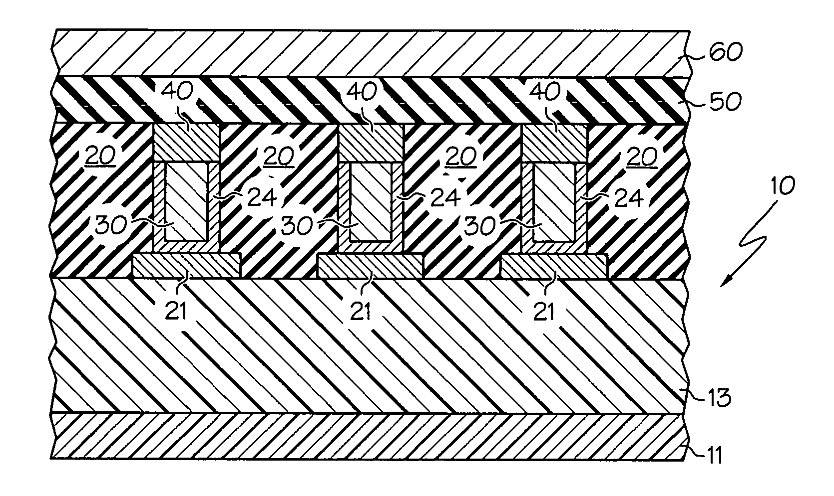
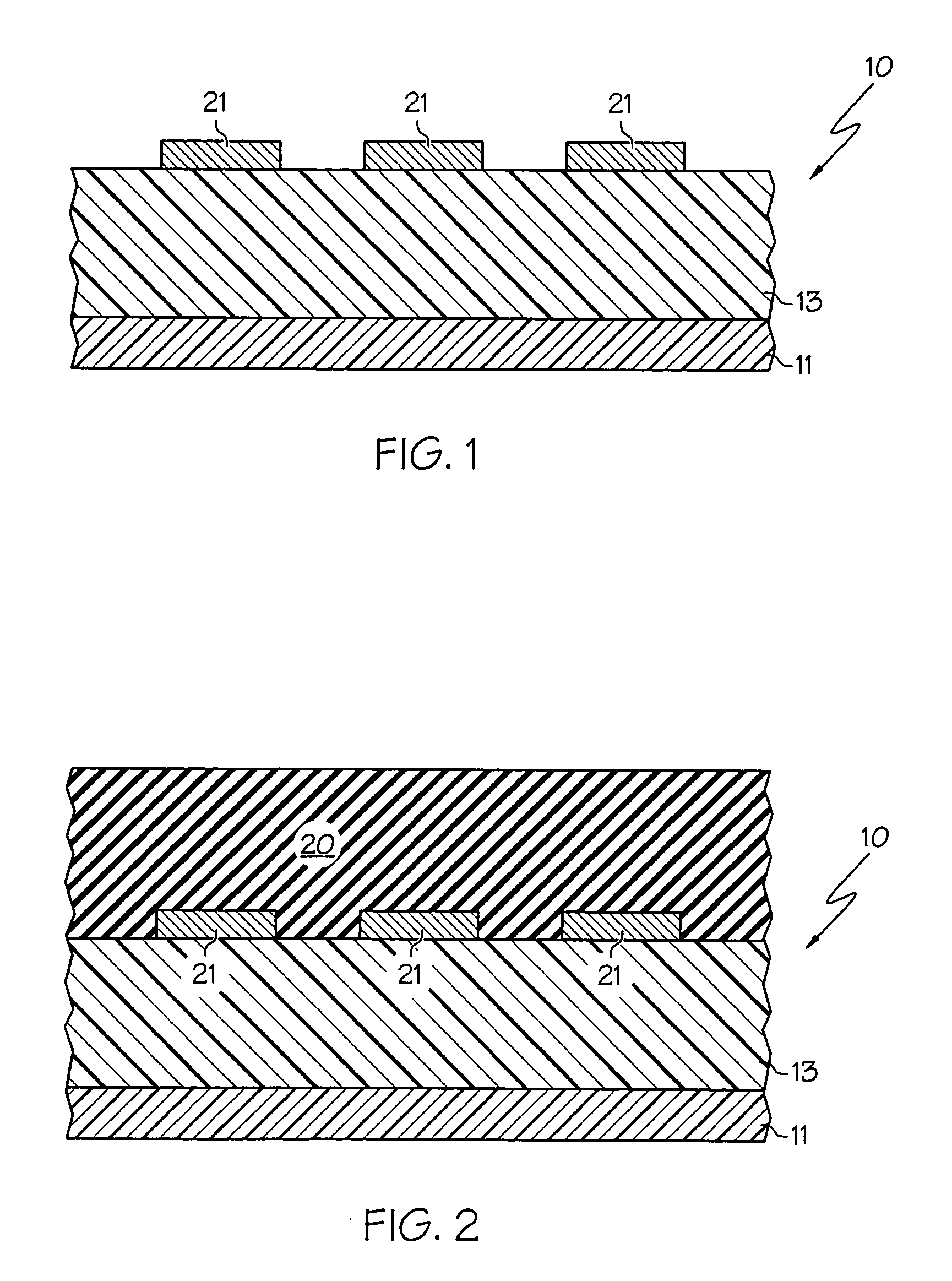
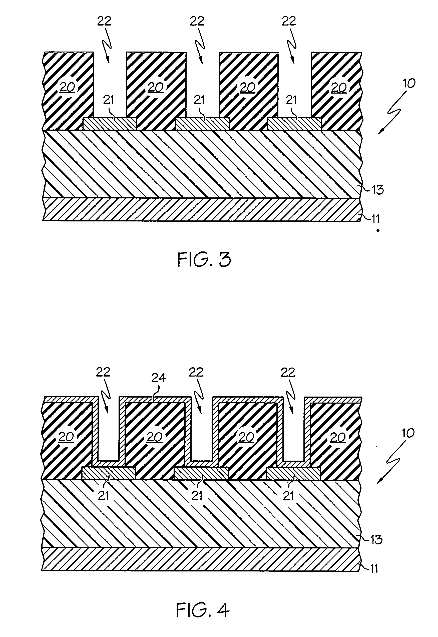
[0026] It is observed that the process steps and structures described herein do not form a complete process flow for manufacturing integrated circuits. Embodiments of the present invention can be practiced in conjunction with a variety of integrated circuit fabrication techniques currently used in the art. As such, commonly practiced process steps are included in the description herein only if those steps are necessary for an understanding of the invention.

[0027] The term “substrate” as used herein may include any semiconductor-based structure that has an exposed semiconductor surface. The term includes structures such as, for example, silicon, silicon-on insulator (SOI), silicon-on sapphire (SOS), doped and undoped semiconductors, epitaxial layers of silicon supported by a base semiconductor foundation, and other semiconductor structures. The semiconductor need not be silicon-based. The semiconductor may be silicon-germanium, or germanium. When reference is made to a “substrate” h...


PUM


Abstract

A method of forming a metal cap over a conductive interconnect in a chalcogenide-based memory device is provided and includes, forming a layer of a first conductive material over a substrate, depositing an insulating layer over the first conductive material and the substrate, forming an opening in the insulating layer to expose at least a portion of the first conductive material, depositing a second conductive material over the insulating layer and within the opening, removing portions of the second conductive material to form a conductive area within the opening, recessing the conductive area within the opening to a level below an upper surface of the insulating layer, forming a cap of a third conductive material over the recessed conductive area within the opening, the third conductive material selected from the group consisting of cobalt, silver, gold, copper, nickel, palladium, platinum, and alloys thereof, depositing a stack of a chalcogenide based memory cell material over the cap, and depositing a conductive material over the chalcogenide stack.

Description

BACKGROUND OF THE INVENTION [0001] The present invention relates to the field of electrochemical deposition, and more particularly to a method of electroless plating a metal cap over a conductive interconnect and to chalcogenide-based memory devices that include such structure. [0002] The performance characteristics and reliability of integrated circuits have become increasingly dependent on the structure and attributes of the vias and interconnects which are used to carry electronic signals between semiconductor devices on integrated circuits or chips. Advances in the fabrication of integrated circuits have resulted in increases in the density, number of semiconductor devices contained on a typical chip, and speed. Interconnect structure and formation technology has not advanced as rapidly, and is increasingly becoming a limitation on the signal speed of integrated circuits. [0003] Present-day, high-performance integrated circuits typically have multiple layers of metal conducting ...

Claims


Application Information

Patent Timeline
IPC IPC(8): H01L21/00H01L21/44
CPCH01L21/288H01L21/76849H01L21/76877H01L45/16H01L45/1233H01L45/143H01L45/085H10N70/245H10N70/8825H10N70/011H10N70/826H01L21/44H01L21/20H10N70/00
Inventor ELKINS, PATRICIA C.MOORE, JOHN T.KLEIN, RITA J.
Owner MICRON TECH INC
Why Eureka
Try Eureka