Method for forming interconnect structure having airgap

a technology of interconnection structure and air gap, which is applied in the direction of electrical apparatus, semiconductor devices, semiconductor/solid-state device details, etc., can solve the problems of severe process integration challenges, difficult to develop a dielectric material with a k value less than 2.5 with good mechanical and suitable integration properties, and all air gap processes require drastic changes to the existing process schemes. to achieve the effect of current process flow

Active Publication Date: 2011-09-08
ASM JAPAN
View PDF9 Cites 292 Cited by
  • Summary
  • Abstract
  • Description
  • Claims
  • Application Information

AI Technical Summary

Benefits of technology

[0006]Consequently, some embodiments of the present invention uses conformal dielectric ALD (atomic layer deposition) process to create airgap spacing, thus reducing Keff without having to further scale down the k value of the bulk dielectric while keeping the current process flow intact or without substantial changes. More specifically, in some embodiments, the dielectric ALD process is performed at a temperature of lower than 400° C. to be compatible with BEOL (back end of line) copper damascene processing. In some embodiments, plasma enhanced ALD (PEALD) is use

Problems solved by technology

However, it has been difficult to develop a dielectric material having a k value of less than 2.5 with good mechanical and suitable integration properties.
In addition, high porosity can lead to connected-pore problems, causing severe process integration challenges (e.g., diffusion problems in ALD/CVD-based metal process technology).
Nevertheless, all of the airgap processes require drastic changes to the existing process schemes.
Although this scheme does not require an additional patterning step fo

Method used


Image

  • Method for forming interconnect structure having airgap
  • Method for forming interconnect structure having airgap
  • Method for forming interconnect structure having airgap

Examples


Embodiment Construction

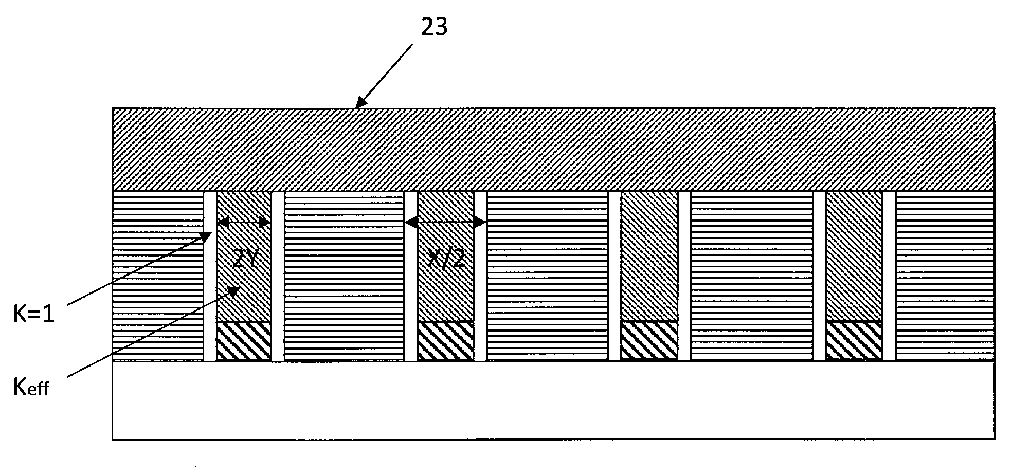
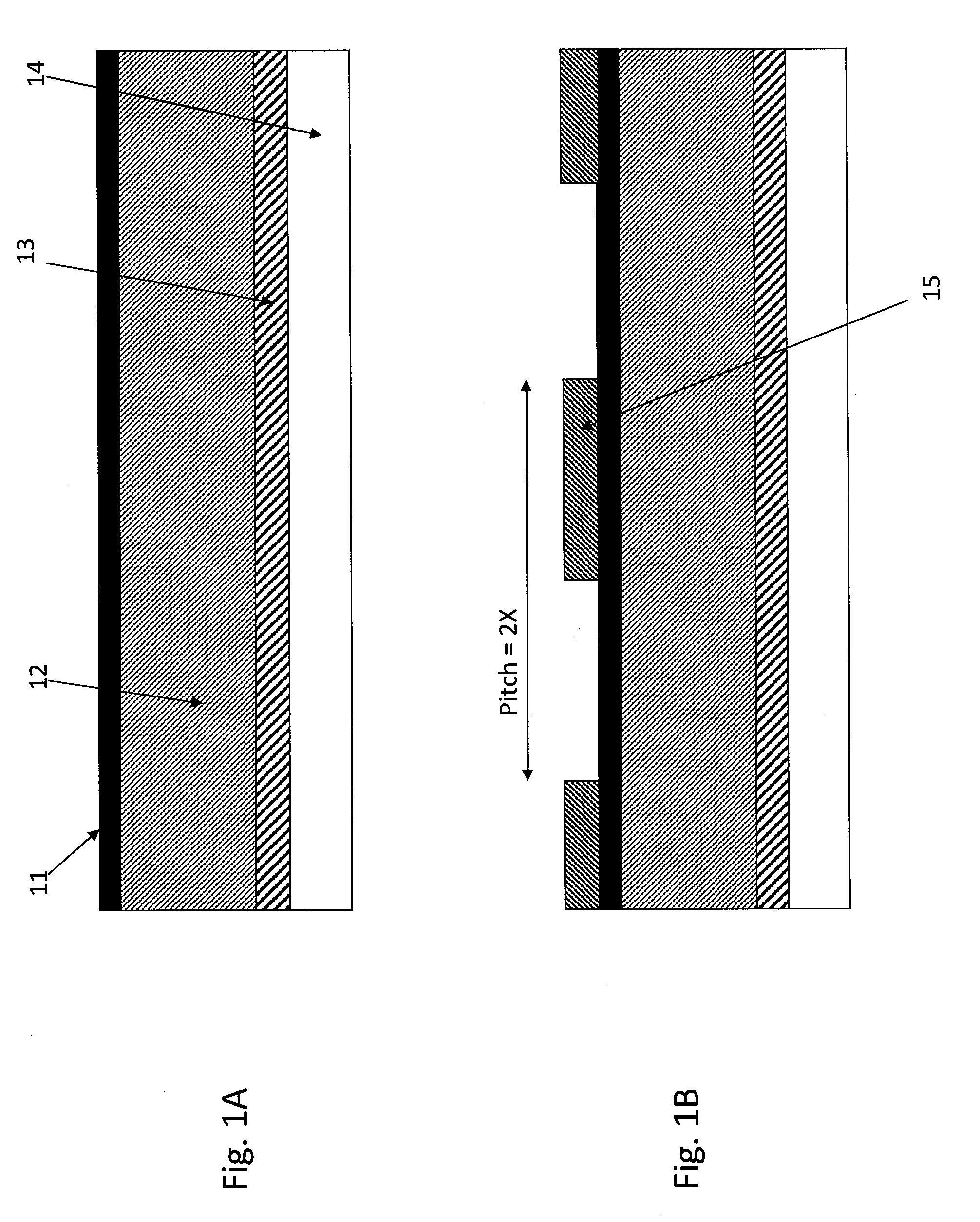
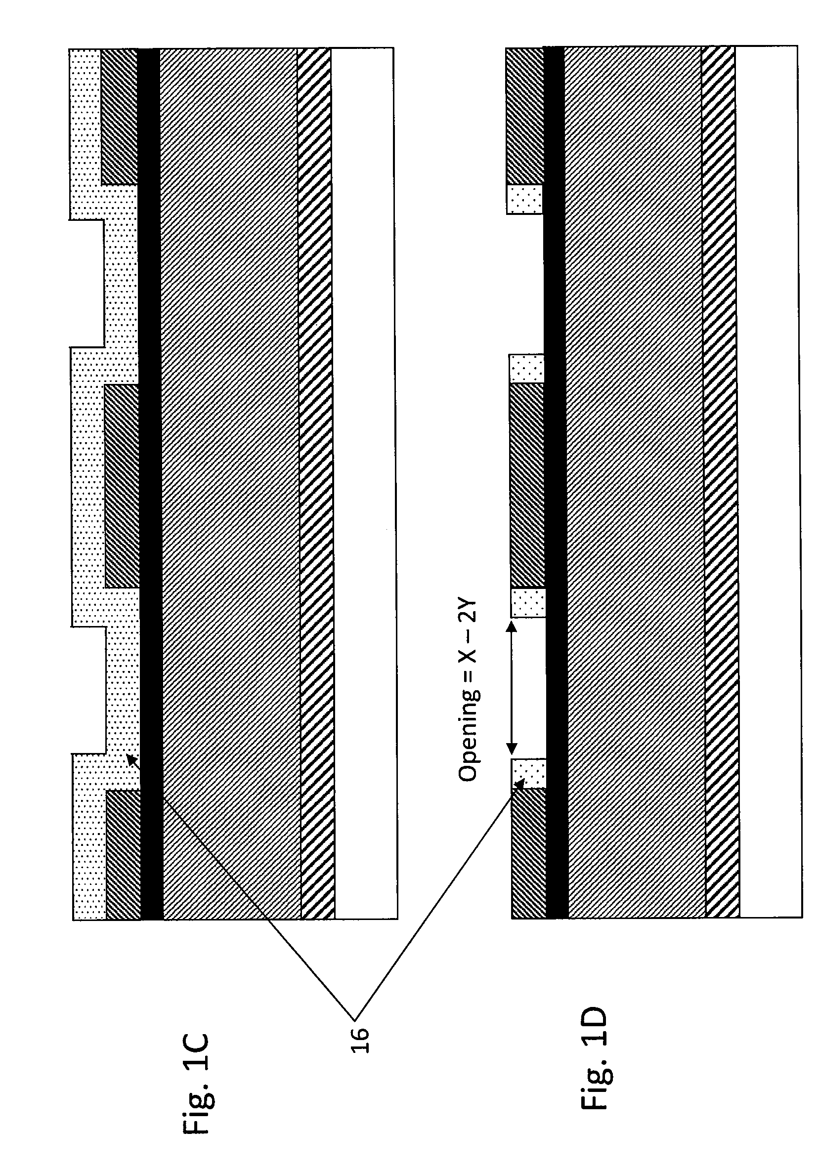
[0022]An embodiment provides a method for forming an interconnect structure with airgaps, comprising: (i) providing a structure having a trench formed on a substrate; (ii) depositing a spacer oxide layer on sidewalls of the trench as sidewall spacers preferably by plasma enhanced atomic layer deposition; (iii) filling the trench having the sidewall spacers with copper; (iv) removing the sidewall spacers to form an airgap structure; and (v) encapsulating the airgap structure, wherein airgaps are formed between the filled copper and the sidewalls of the trench.

[0023]In some embodiments, the method may further comprise depositing a SiCxNy-based spacer layer (hereinafter in “SiCxNy”, x and y indicate a type of film, rather than indicating actual atomic compositions, and are independently 0 or 1, typically both x and y are 1) on the sidewall spacers by atomic layer deposition before filling the trench, wherein airgaps are formed between the SiCxNy-based spacer layer and the sidewalls of ...


PUM


Abstract

A method for forming an interconnect structure with airgaps, includes: providing a structure having a trench formed on a substrate; depositing a spacer oxide layer on sidewalls of the trench as sidewall spacers by plasma enhanced atomic layer deposition; filling the trench having the sidewall spacers with copper; removing the sidewall spacers to form an airgap structure; and encapsulating the airgap structure, wherein airgaps are formed between the filled copper and the sidewalls of the trench.

Description

BACKGROUND[0001]1. Field of the Invention[0002]The present invention generally relates to a method for forming interconnect structures, particularly to a method for forming interconnect structures having airgaps.[0003]2. Description of the Related Art[0004]As the dimension between metal lines decreases for each successive technology node, it is necessary to continue scaling down the capacitance between metal lines to reduce cross-talk and RC delay. Towards this objective, the k value (dielectric constant) of dielectric materials has been scaled down aggressively in the past decade from 4.0 to about 2.5. Leading edge manufacturing companies have recently reached a Keff of about 2.7 (effective k value) with the use of low-k CDO (carbon doped oxide) having a k value of about 2.5 and SiCN dielectric diffusion barrier having a k value of about 5.0. In order to achieve scaling Keff significantly below 2.5, a further decrease of k value from 2.5 to less than 2.3 will be required. The ITRS ...

Claims


Application Information

Patent Timeline
IPC IPC(8): H01L21/768
CPCH01L21/768H01L21/7682H01L21/76831H01L23/53295H01L23/53238H01L2221/1063H01L2924/0002H01L2924/00H01L21/76834H01L23/5222
Inventor HSIEH, JULIAN J.KOBAYASHI, NOBUYOSHISHIMIZU, AKIRAMATSUSHITA, KIYOHIROFUKAZAWA, ATSUKI
Owner ASM JAPAN
Why Eureka
Try Eureka