
Cleaning of carbon-based contaminants in metal interconnects for interconnect capping applications

Inactive Publication Date: 2015-12-31
LAM RES CORP
View PDF13 Cites 294 Cited by
  • Summary
  • Abstract
  • Description
  • Claims
  • Application Information

AI Technical Summary

Benefits of technology

The patent text describes a process where a dielectric layer is treated with a substance called a silylating agent. This treatment makes the dielectric layer resistant to another substance called a capping material, which is used in semiconductor manufacturing. As a result, the process becomes more selective, meaning it can deposit the capping material without depositing other materials on the same layer.

Problems solved by technology

One challenging problem encountered during IC fabrication is contamination of metal line surfaces with carbon-containing residue.
Presence of such contamination can hinder the deposition of caps on metal lines.
For example, when metal-containing caps, such as cobalt-containing caps or manganese-containing caps are deposited by chemical vapor deposition (CVD) or atomic layer deposition (ALD) on a surface contaminated with carbon, low deposition rates, patchy and uneven deposition may result.
In many instances, presence of carbon-based contaminants on the surface of the metal line reduces selectivity of such deposition.
While contamination with oxide species, such as with copper oxide can be readily removed by treatment of the substrate with reducing agents (e.g., by plasma or thermal treatment in a reducing atmosphere), contamination with carbon-containing species is generally not easily treated.

Method used


Image

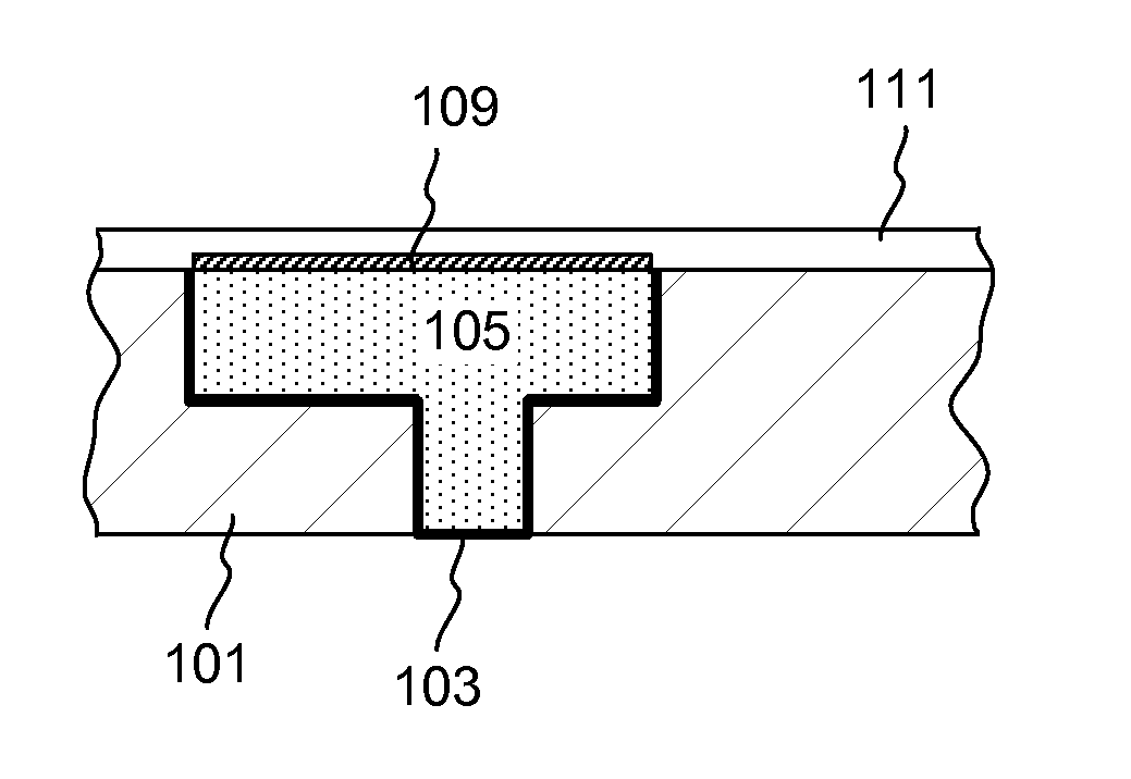
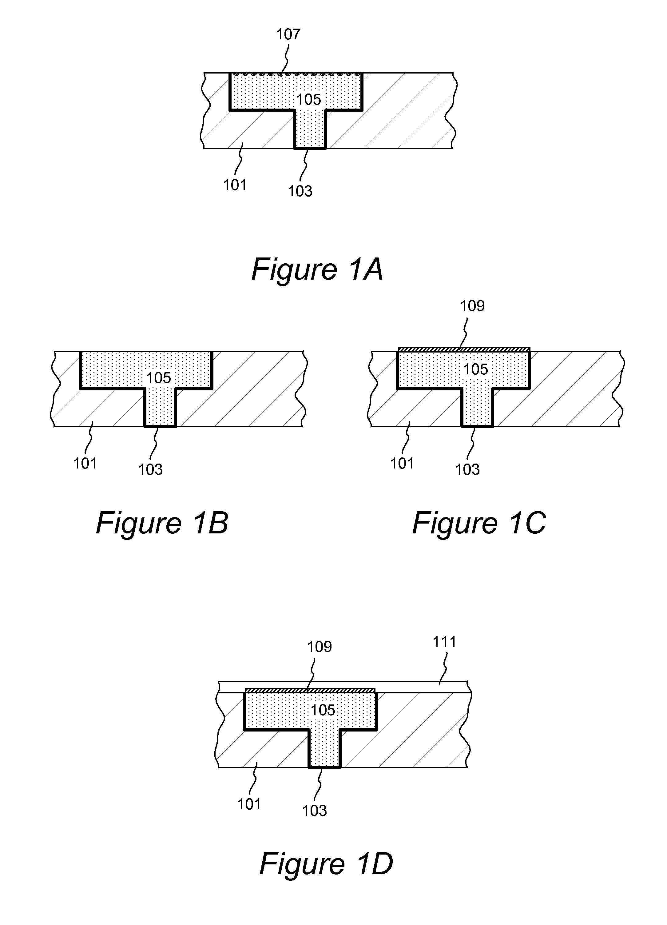
  • Cleaning of carbon-based contaminants in metal interconnects for interconnect capping applications
  • Cleaning of carbon-based contaminants in metal interconnects for interconnect capping applications
  • Cleaning of carbon-based contaminants in metal interconnects for interconnect capping applications

Examples


experimental examples

Example 1

[0053]X-Ray Photoelectron spectroscopic (XPS) data was obtained on thin copper films deposited and processed by different methods. FIG. 4A shows XPS data for a thin copper film deposited by electroplating and planarized by CMP. Two peaks assigned to carbon-containing contaminants were observed in this sample: a peak at about 289 eV is assigned to a carbon-oxygen (carbonate) bonding and a peak at about 285 eV assigned to C—C or C—H bonding. FIG. 4B shows XPS data for a thin copper film deposited by PVD that was not subjected to subsequent CMP treatment. Two peaks assigned to carbon-containing contaminants were also observed in this sample: a peak at about 289 eV is assigned to a carbon-oxygen (carbonyl) bonding and a peak at about 285 eV assigned to C—C or C—H bonding. Both graphs refer to C1s XPS data. These data illustrate that carbon-containing contaminants are present on copper layer deposited by different methods, and are not limited to contamination derived from chemic...

example 2

[0054]Carbon and silicon content was measured by XPS (using integrated areas of C1s and Si2p peaks respectively) in different samples of copper layers treated with a silylating agent under different conditions. Graph shown in FIG. 5 illustrates dependence of silicon content (y-axis) on total carbon content (x-axis). Two series of data were obtained. The series shown in diamonds refers to the samples of electrodeposited CMP-treated copper. The series shown in squares refers to the samples of PVD-deposited copper that was not planarized by CMP. It can be seen that in both series the carbon and silicon content are positively correlated, suggesting a binding between the carbon-containing contaminants and the silylation agent.

example 3

[0055]XPS data for carbon (C1s) were obtained on a sample containing a copper layer before and after treatment with a silylating agent, where the treatment included heating to remove the reacted silylating agent. The intensity of peaks at about 285 eV and 289 eV was substantially reduced.


PUM

PropertyMeasurementUnit
Temperatureaaaaaaaaaa
Pressureaaaaaaaaaa

Abstract

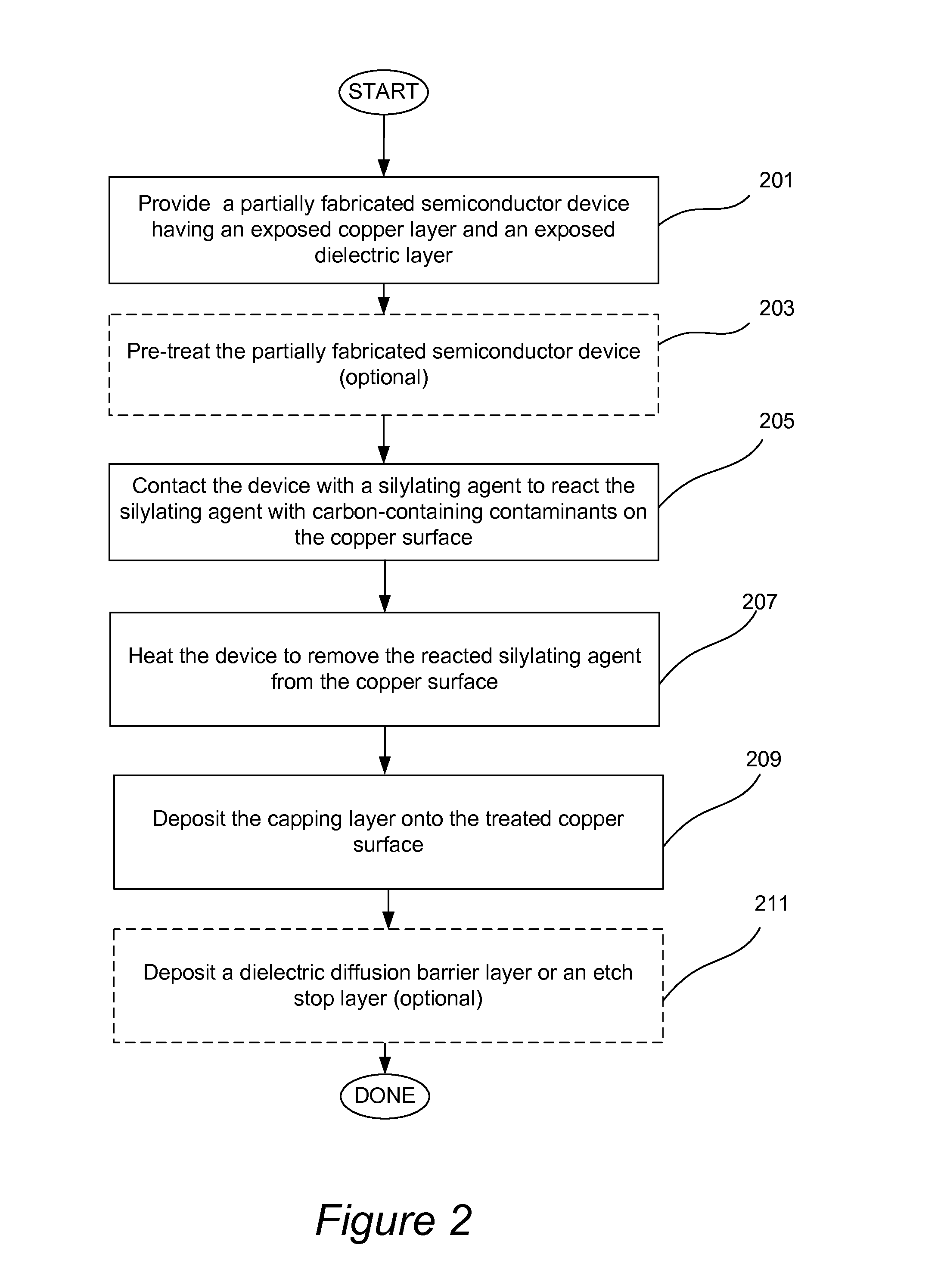
Protective caps residing at an interface between copper lines and dielectric diffusion barrier layers are used to improve various performance characteristics of interconnects. The caps, such as cobalt-containing caps or manganese-containing caps, are selectively deposited onto exposed copper lines in a presence of exposed dielectric using CVD or ALD methods. The deposition of the capping material is affected by the presence of carbon-containing contaminants on the surface of copper, which may lead to poor or uneven growth of the capping layer. A method of removing carbon-containing contaminants from the copper surface prior to deposition of caps involves contacting the substrate containing the exposed copper surface with a silylating agent at a first temperature to form a layer of reacted silylating agent on the copper surface, followed by heating the substrate at a higher temperature to release the reacted silylating agent from the copper surface.

Description

FIELD OF THE INVENTION[0001]The present invention pertains to methods of forming layers of material on a partially fabricated integrated circuit. Specifically, the invention pertains to methods of cleaning carbon-based contaminants in metal interconnects for interconnect capping applications.BACKGROUND OF THE INVENTION[0002]Damascene processing is a method for forming metal lines on integrated circuits. It involves formation of inlaid metal lines in trenches and vias formed in a dielectric layer (inter layer dielectric). Damascene processing is often a preferred method because it requires fewer processing steps than other methods and offers a higher yield. It is also particularly well-suited to metals such as copper that cannot be readily patterned by plasma etching.[0003]In a typical Damascene process, metal is deposited onto a patterned dielectric to fill the vias and trenches formed in the dielectric layer. The resulting metallization layer is typically formed either directly on ...

Claims


Application Information

Patent Timeline
IPC IPC(8): H01L21/768C23C16/02C23C16/52
CPCH01L21/76883H01L21/28556H01L21/76826C23C16/16H01L21/76849H01L21/02074C23C16/0227H01L21/76834H01L21/02057H01L21/67011
Inventor ANTONELLI, GEORGE ANDREWKNISLEY, THOMAS JOSEPHSUBRAMONIUM, PRAMOD
Owner LAM RES CORP
Learn More