Surface acoustic wave device

a surface acoustic wave and device technology, applied in piezoelectric/electrostrictive/magnetostrictive devices, piezoelectric/electrostriction/magnetostriction machines, impedence networks, etc., can solve the problems of electrical breakage, electrode breakage, and strong stress on the surface acoustic wave, so as to reduce the loss of insertion elements, enhance the q-factor of resonators, and suppress the effect of stress

Active Publication Date: 2007-02-20
QORVO US INC
View PDF5 Cites 7 Cited by
  • Summary
  • Abstract
  • Description
  • Claims
  • Application Information

AI Technical Summary

Benefits of technology

[0016]The present invention has been made in order to solve the problems in the prior arts, and it is an object of the present invention to provide a surface acoustic wave device which can enhance withstand power.
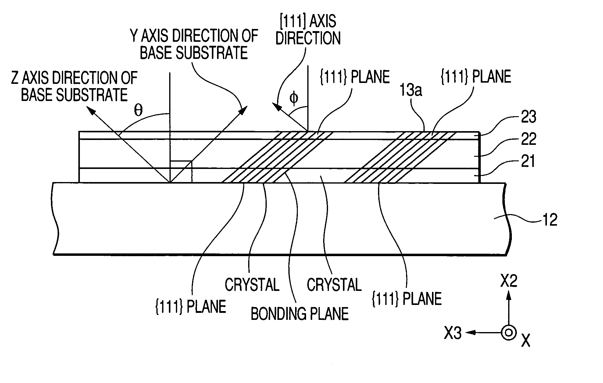
[0018]According to the present invention, the main electrode layer of the face-centered cubic structure is deposited on the base layer of the rock-salt structure, the face-centered cubic structure, or the hexagonal closest-packed structure such that the {111} plane as a closest-packed plane of the main electrode layer has the constant gradient with respect to the substrate surface. Thus, the electromigration or stress migration can be suppressed. As a result, an electrode breakage and electrical breaks can be prevented, an insertion loss of elements can be decreased, and a Q-factor of resonators can be increased. Therefore, properties of the surface acoustic wave device can be enhanced.
[0019]Further, when the {111} plane of the main electrode layer is parallel to an X-axis of crystals of the piezoelectric substrate, the {111} plane as the closest-packed plane crosses an amplitude direction of shear horizontal (SH) waves. Thus, resistance to electromigration or stress migration can be enhanced.
[0030]Further, when the piezoelectric substrate is made of LiTaO3 having a Y-cut angle ranging from 36° to 60°, resonance property of the surface acoustic wave device is enhanced.
[0032]Further, when a protective layer made of TiN (titanium nitride) or TiOxNy (where 0<x<0.2, x+y=1) is deposited on the main electrode layer, the crystal structure of the main electrode layer can be stabilized and resistance to electromigration or stress migration can be enhanced.
[0034]According to the present invention, the main electrode layer of the face-centered cubic structure is deposited on the base layer of the rock-salt structure, the face-centered cubic structure, or the hexagonal closest-packed structure such that the {111} plane as the closest-packed plane of the main electrode layer has the constant gradient with respect to the substrate surface. Thus, the electromigration or stress migration can be suppressed. As a result, even if the operating frequency of the surface acoustic wave device increases from several hundred MHz to several GHz, the electrode breakage and the electrical breaks can be prevented, the insertion loss of elements can be decreased, and the Q-factor of resonators can be enhanced. Therefore, the properties of the surface acoustic wave device can be enhanced.

Problems solved by technology

When high-voltage signals are applied to the interdigital electrodes having such fine electrode fingers, the interdigital electrodes suffer from strong stress due to surface acoustic waves.
The electromigration or stress migration causes a breakage of the electrodes, electrical breaks, an increase in insertion loss of elements, a decrease in Q-factor of resonators, and the like, and finally causes deterioration of the surface acoustic wave device.
This causes a breakage of the electrodes, electrical breaks, an increase in insertion loss of elements, a decrease in Q-factor of resonators, and the like, and finally causes deterioration of the surface acoustic wave device.
Therefore, there is a problem in that the electrical resistance of the interdigital electrode section becomes large, thereby increasing the insertion loss of elements.
However, in this prior art, an example of a surface acoustic wave device, in which the layer made of TiN is formed below the layer made of the Al alloy, and the rules for liquid crystal orientation are not disclosed.

Method used


Image

  • Surface acoustic wave device
  • Surface acoustic wave device
  • Surface acoustic wave device

Examples


example 1

[0140]The Al alloy layer (the main electrode layer) made of an AlScCu alloy is film-formed on the piezoelectric substrate made of LiTaO3 having the Y-cut angle of 46° through the base layer by means of the sputter method. FIG. 5 is an expanded photograph of the interdigital electrode section of the surface acoustic wave device according to an example 1 in which the base layer is formed with TiN, as viewed from a cross-section orthogonal to the X-axis of the LiTaO3 substrate. FIG. 6 is a partial side view schematically showing the interdigital electrode section shown in FIG. 5. FIG. 7 is an expanded photograph showing an interdigital electrode section of a surface acoustic wave device according to a comparative example 1 in which the base layer is formed with Ti, and FIG. 8 is an expanded photograph showing an interdigital electrode section of a surface acoustic wave device according to a comparative example 2 in which the base layer is formed with Mo. FIGS. 9 and 10 are partial side...


PUM


Abstract

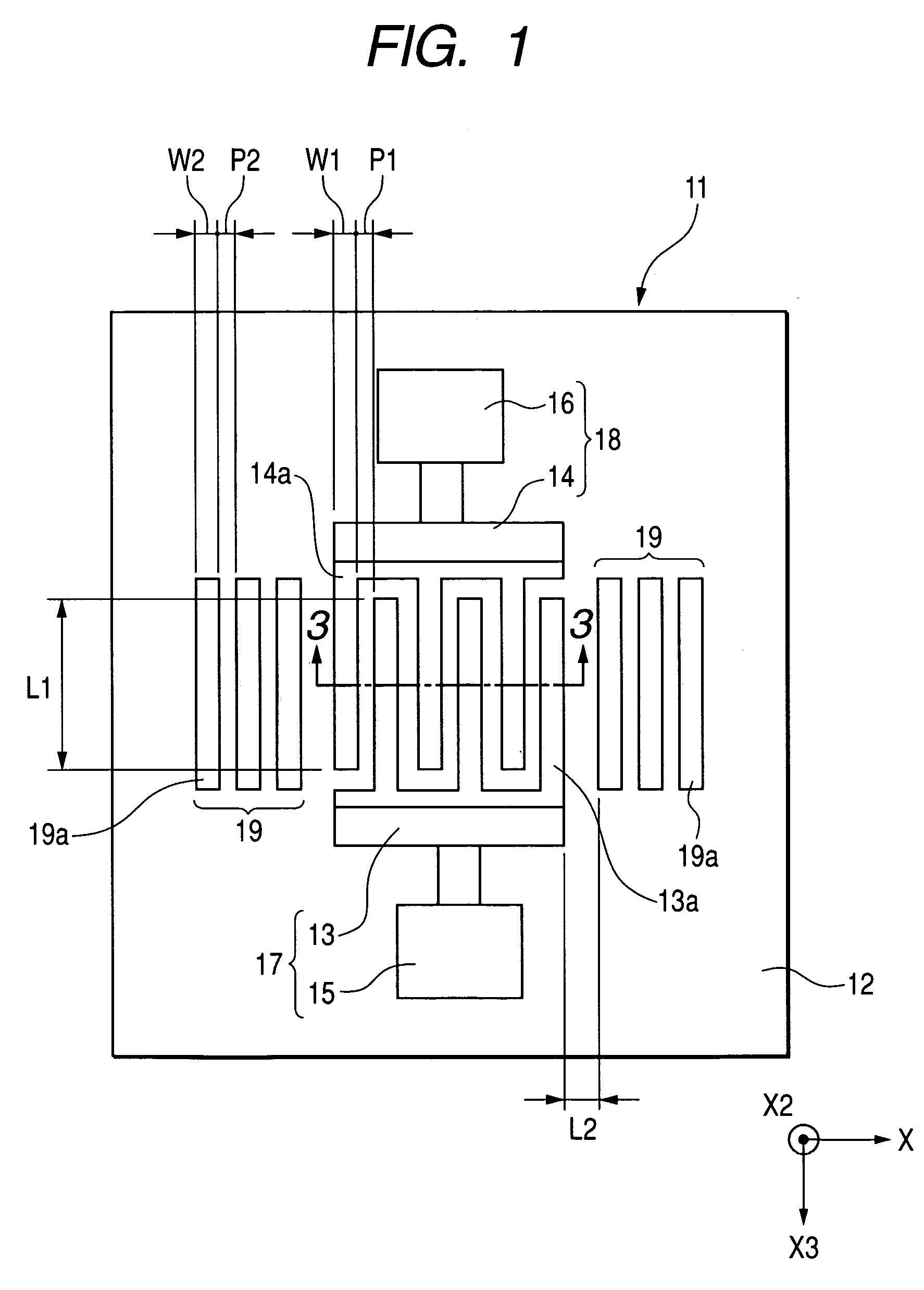
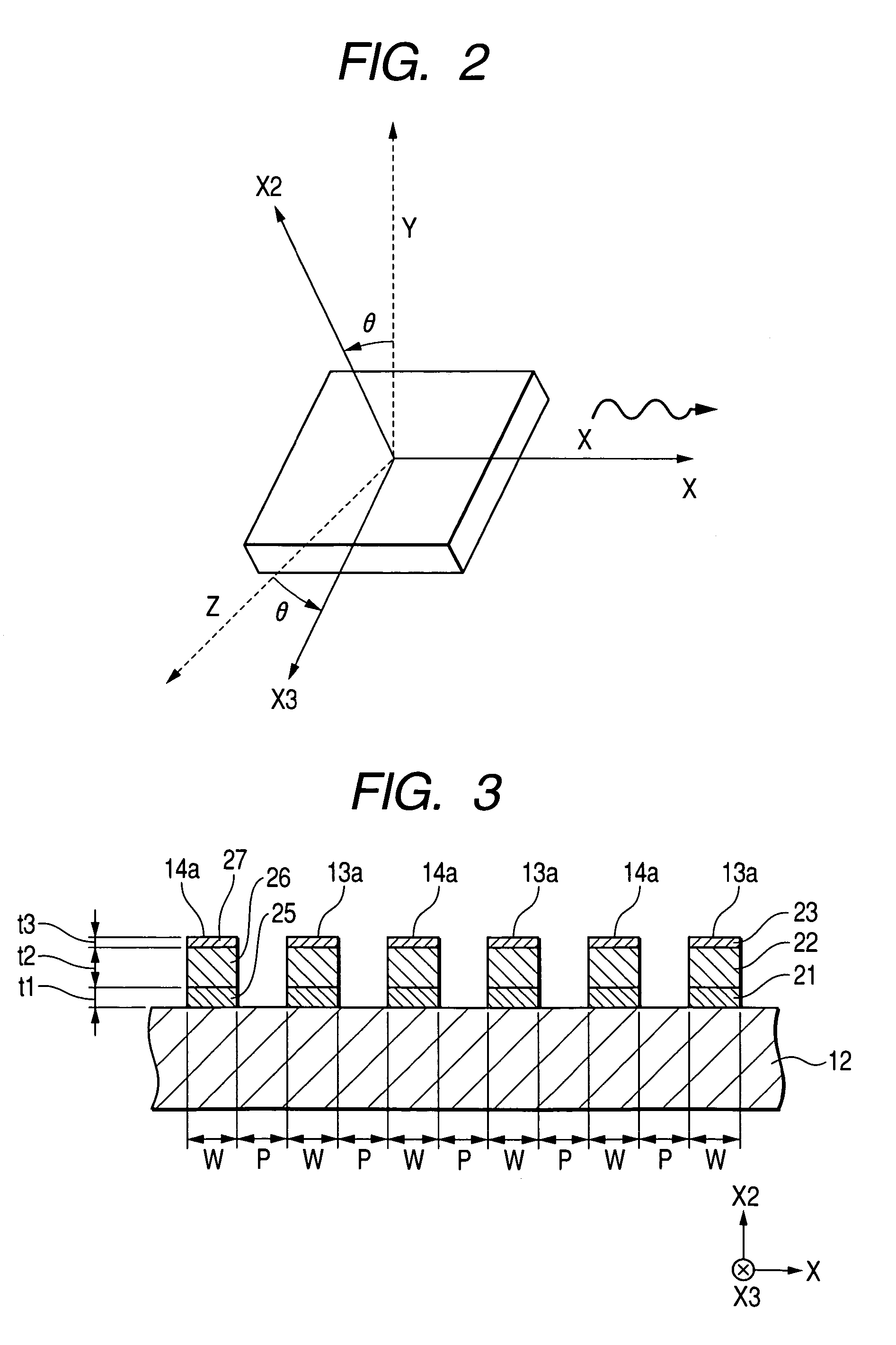
There is provided a surface acoustic wave device which can prevent a breakage of electrodes and electrical breaks, decrease an insertion loss of elements, and enhance a Q-factor of resonators. Interdigital electrode sections and each have a laminated structure of a base layer made of TiN (titanium nitride) or TiOxNy and a main electrode layer deposited to come in contact with an upper surface of the base layer. The main electrode layer is deposited such that a {111} plane as a closest-packed plane of the main electrode layer has a constant gradient with respect to a surface of a substrate, and thus electromigration or stress migration can be suppressed in the interdigital electrode sections.

Description

[0001]This application claims the benefit of priority to Japanese Patent Application Nos. 2004-030211 filed on Feb. 6, 2004 and 2004-147241 filed on May 18, 2004, both herein incorporated by reference.BACKGROUND OF THE INVENTION[0002]1. Field of the Invention[0003]The present invention relates to a surface acoustic wave device having an electrode structure with high withstand power at high frequencies.[0004]2. Description of the Related Art[0005]Surface acoustic wave devices are electronic components using surface acoustic waves, which are mechanical vibrations propagating along surfaces of solid materials, and they are used for filters, resonators, or duplexers.[0006]Recently, the miniaturization of mobile communication terminals such as cellular phones has been advancing. Therefore, electronic components of such terminals must be reduced in size.[0007]A surface acoustic wave device has a piezoelectric substrate and a pair of interdigital electrodes (interdigital transducer (IDT) e...

Claims


Application Information

Patent Timeline
Patent Type & Authority Patents(United States)
IPC IPC(8): H01L41/08H03H3/08H03H9/02H03H9/145
CPCH03H3/08H03H9/14541H03H9/02929H03H9/02559
Inventor OZAKI, KYOSUKESASAKI, MAKOTOFUJIMOTO, HARUHIKOWAGA, SATOSHI
Owner QORVO US INC
Why Eureka
Try Eureka