Display apparatus and method of manufacturing the same

a display device and display technology, applied in the direction of discharge tubes, luminescent screens, identification means, etc., can solve the problems of damage to the drive circuit, the display performance of the organic el device cannot be maintained as a display device, and the organic el device is very susceptible to moisture, so as to enhance reliability and process precision

Active Publication Date: 2007-03-20
JAPAN DISPLAY CENTRAL CO LTD
View PDF16 Cites 49 Cited by
  • Summary
  • Abstract
  • Description
  • Claims
  • Application Information

AI Technical Summary

Benefits of technology

[0010]The present invention has been made to solve the above problems, and the object of the invention is to provide a display apparatus capable of enhancing reliability and process precision, and a method of manufacturing the display apparatus.

Problems solved by technology

The organic EL device is very susceptible to moisture.
Even a small amount of moisture, e.g. about 1 ppm, would destroy the organic EL device, and the organic EL device could no longer maintain a display performance as a display device.
This may result in damage to the drive circuit.
In particular, in display apparatuses used in small-sized mobile terminals, the production of which has increased in recent years, there is little extra area in the frame size and thus it is difficult to keep a sufficient margin.
Consequently, the aforementioned problem tends to occur with the display apparatus for the small-sized mobile terminal, and the reliability may deteriorate.
As a result, defects such as a chip tend to occur at end portions of the substrates of the cut-out organic EL display apparatuses, and it is difficult to cut out the display apparatuses with high precision.

Method used


Image

  • Display apparatus and method of manufacturing the same
  • Display apparatus and method of manufacturing the same
  • Display apparatus and method of manufacturing the same

Examples


Embodiment Construction

[0034]A display apparatus according to an embodiment of the present invention and a method of manufacturing the display apparatus will now be described with reference to the accompanying drawings.

[0035]In this embodiment, a self-emission type display apparatus, such as an organic EL (electroluminescence) display apparatus, is described as the display apparatus by way of example.

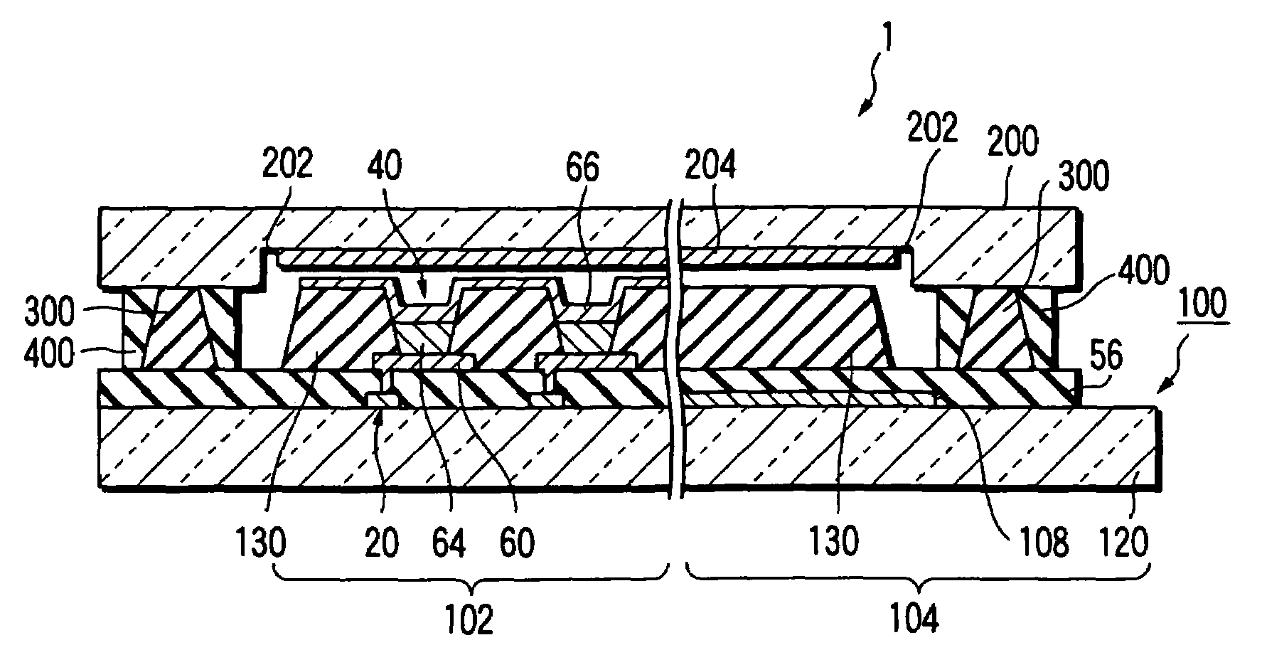
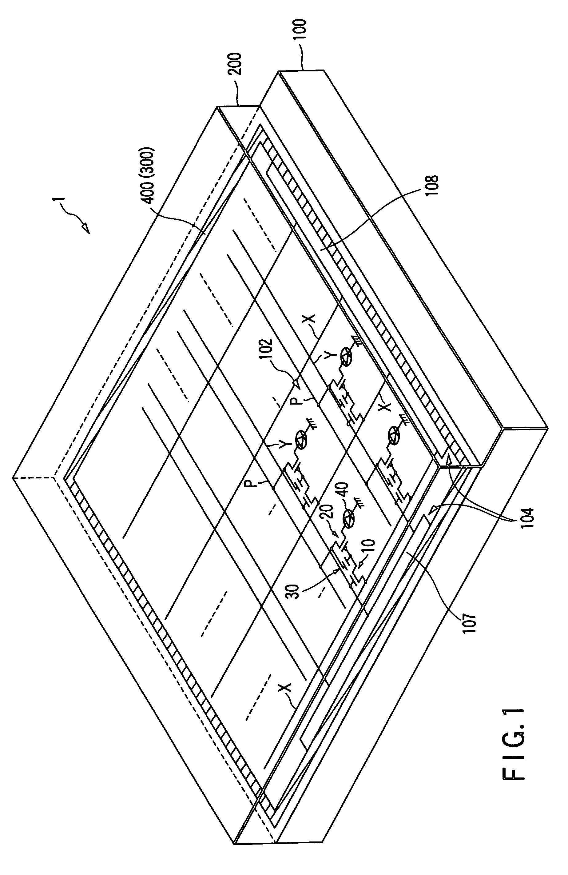
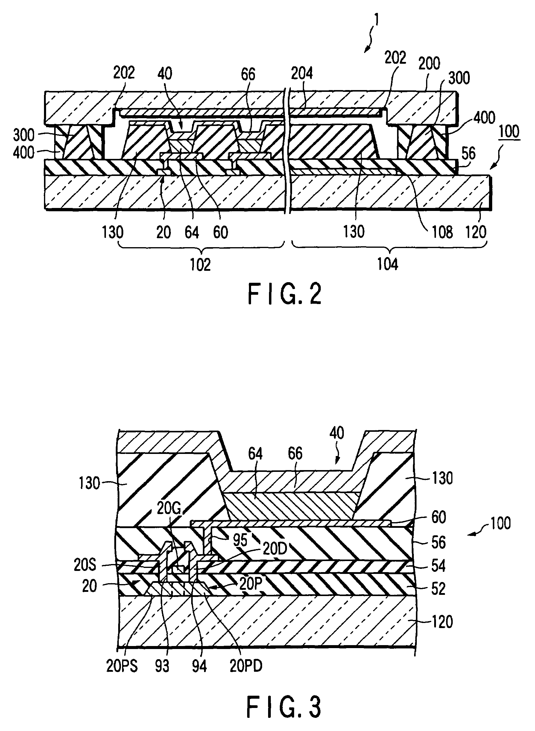
[0036]As is shown in FIG. 1 and FIG. 2, an organic EL display apparatus 1 comprises an array substrate 100 as a first substrate, on which organic EL devices serving as display devices are arranged in a matrix, and a sealing substrate 200 as a second substrate, which is disposed to be opposed to the array substrate 100. A display area 102 of the array substrate 100, which displays an image, comprises three kinds of light-emitting portions, that is, pixels, which emit red, green and blue lights, respectively. Each pixel is separated by separators 130. Each pixel includes an organic EL device 40 serving as a sel...


PUM


Abstract

A display apparatus includes an array substrate including a display area composed of a plurality of pixels arranged in a matrix, and a sealing substrate disposed to be opposed to the array substrate. The display area includes a pixel switch that selects a pixel, a drive control device connected to the pixel switch, and an organic EL device driven by the drive control device. A support section is disposed in a frame shape on an outer peripheral portion of the display area such that a predetermined gap is provided between the array substrate and the sealing substrate.

Description

CROSS-REFERENCE TO RELATED APPLICATIONS[0001]This is a Continuation Application of PCT Application No. PCT / JP03 / 01017, filed Jan. 31, 2003, which was not published under PCT Article 21(2) in English.[0002]This application is based upon and claims the benefit of priority from the prior Japanese Patent Application No. 2002-027123, filed Feb. 4, 2002, the entire contents of which are incorporated herein by reference.BACKGROUND OF THE INVENTION[0003]1. Field of the Invention[0004]The present invention relates to a display apparatus and a method of manufacturing the display apparatus, and more particularly to a self-emission type display apparatus such as an organic electro-luminescence (EL) display apparatus and a method of manufacturing the same.[0005]2. Description of the Related Art[0006]In recent years, organic EL display apparatuses have attracted attention as flat display apparatuses. The organic EL display apparatus has self-luminescence properties. Thus, it has features: a wide ...

Claims


Application Information

Patent Timeline
Patent Type & Authority Patents(United States)
IPC IPC(8): H05B33/04H01L51/00G09F9/00G09F9/30G09G3/32H01L27/32H01L51/50H01L51/52H01L51/56H05B33/22H05B44/00
CPCH01L51/5237H01L27/3246G09G3/3208G09G3/3225G09G2300/0842H01L2251/566H01L51/56H10K59/122H10K50/8428H10K50/846H10K50/8426H10K71/851H10K71/00H05B33/04
Inventor TOMIMATSU, TOSHIFUMIKOBAYASHI, MICHIYA
Owner JAPAN DISPLAY CENTRAL CO LTD
Why Eureka
Try Eureka