Image sensor module and fabrication method thereof

a technology of image sensor and fabrication method, which is applied in the direction of instruments, semiconductor/solid-state device details, radio-controlled devices, etc., can solve the problems of image darkening, increased fabrication cost, and overlapping of expensive aspheric lenses, so as to improve efficiency and precision, the effect of reducing the fabrication cos

Active Publication Date: 2009-05-07
SAMSUNG ELECTRONICS CO LTD
View PDF15 Cites 137 Cited by
  • Summary
  • Abstract
  • Description
  • Claims
  • Application Information

AI Technical Summary

Benefits of technology

[0009]Exemplary embodiment of the present invention addresses at least the above aspects. Accordingly, an aspect of the present invention is to provide an image sensor module having a sensor chip-mounting structure capable of improving efficiency and precision for forming a concave surface on which a sensor chip is bent and bonded, thereby reducing fabrication cost, and a fabrication method thereof.

Problems solved by technology

However, a conventional typical image sensor module is configured, so that to calibrate an aberration caused by discordance between a focal plane of lens in the form of a curved surface and a sensor surface of a sensor chip in the form of a plane, a plurality of expensive aspheric lenses lies one upon another.
Thus, the conventional image sensor module comes large in whole thickness, does not obtain sufficient high resolution, and causes fabrication costs to increase.
Thus, the conventional image sensor module presents a vignetting phenomenon that as pixels located at an edge of the sensor chip decrease in the intensity of received irradiation, images are become dark.
In this case, however, the image sensor module does not only come large in whole thickness, but also does not act to calibrate the intensity of received irradiation if it is operated to use a zoom function.
If the image sensor module is fabricated in a level of single part, however, it presents a problem in that when bonding the thinned sensor chips on corresponding concave surfaces of a silicon substrate one by one, it is difficult to precisely align the thinned sensor chips with the corresponding concave surfaces.
In addition, if the image sensor module is fabricated in a wafer level, it presents a problem in that it is difficult to fabricate the concave surfaces to coincide with a pitch in an array of sensor chips through a conventional machining method and it is difficult or impossible to form metal via interconnections for electrical connection to penetrate the silicon substrate.

Method used


Image

  • Image sensor module and fabrication method thereof
  • Image sensor module and fabrication method thereof
  • Image sensor module and fabrication method thereof

Examples


Embodiment Construction

[0046]Reference will now be made in detail to an exemplary embodiment of the present invention, which are illustrated in the accompanying drawings, wherein like reference numerals refer to the like elements throughout. The exemplary embodiment is described below in order to explain the present invention by referring to the figures.

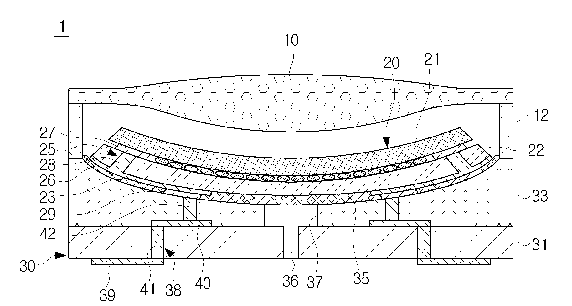
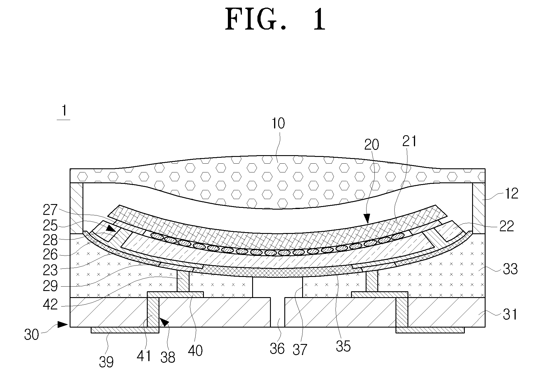
[0047]FIG. 1 is a cross-sectional view exemplifying an image sensor module 1 in accordance with an exemplary embodiment of the present invention.

[0048]As illustrated in FIG. 1, the image sensor module 1 in accordance with the exemplary embodiment of the present invention includes a lens 10, a sensor chip 20, and a sensor chip-mounting structure 30.

[0049]The lens 10 is made up of a low-priced spherical surface lens, and adhered and supported on the sensor chip-mounting structure 30 by a spacer 12, which is formed of a silicon or plastic material. The spacer 12 may be formed by etching a silicon wafer or injection-molding a plastic material.

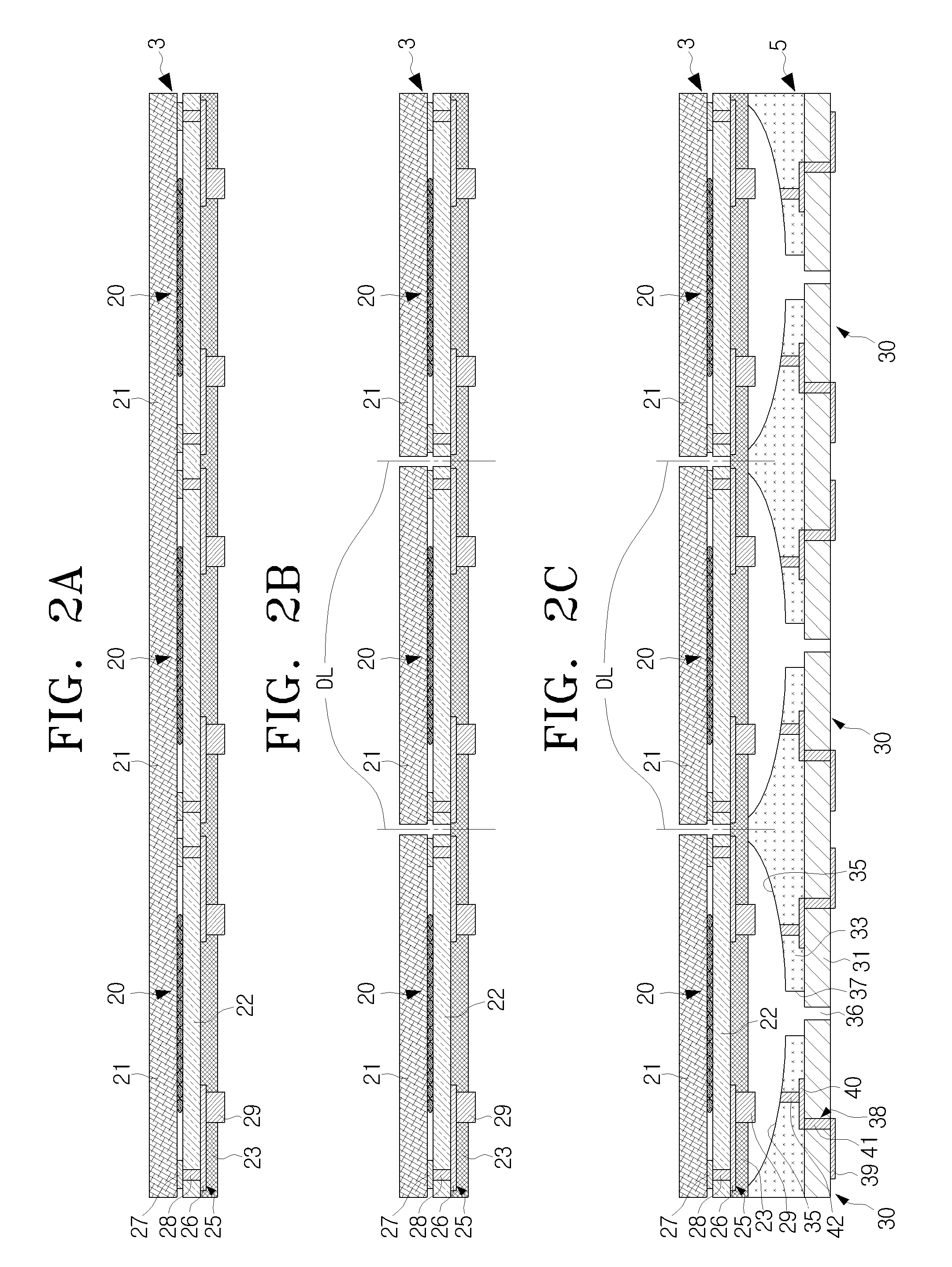
[0050]The sensor ...


PUM


Abstract

An image sensor module having a sensor chip closely adhered on a concave surface and a fabrication method thereof are disclosed. The image sensor module includes at least one sensor chip, at least one sensor chip-mounting structure comprising a substrate and a polymer layer formed on the substrate, the polymer layer having an concave surface formed on an upper part thereof by a polymer molding method, so that the sensor chip is bent and bonded on the concave surface, and at least one lens fixed on the at least one sensor chip-mounting structure above the sensor chip.

Description

CROSS-REFERENCE TO RELATED PATENT APPLICATION[0001]This application claims priority from Korean Patent Application No. 10-2007-0111185 filed on Nov. 1, 2007 in the Korean Intellectual Property Office, the disclosure of which is incorporated herein by reference.BACKGROUND OF THE INVENTION[0002]1. Field of the Invention[0003]Apparatuses and methods consistent with the present invention relate to an image sensor module, which is used in an electronic device, such as a camera phone, a digital camera, etc. More particularly, the present invention relates to an image sensor module having a sensor chip closely adhered on a concave surface, and a fabrication method thereof.[0004]2. Description of the Related Art[0005]Generally, an electronic device, such as a camera phone, a digital camera, etc., has an image sensor module, which can take a photograph of a certain object. The image sensor module requires satisfying conditions including miniaturization, high resolution, and thinness, as well...

Claims


Application Information

Patent Timeline
Patent Type & Authority Applications(United States)
IPC IPC(8): H04N5/335H01L31/0232
CPCH01L27/14618H01L27/14683H04N5/3696H04N5/2257H04N5/335H04N5/2253H01L24/97H01L2224/16H01L2924/3511H01L2924/15788H01L27/14632H01L27/14687H04N23/54H04N23/57H04N23/55H04N25/00H01L2924/00H01L27/146
Inventor CHOI, MIN-SEOGLEE, SEUNG-WANKIM, WOON-BAELEE, EUN-SUNGJUNG, KYU-DONGKIM, CHE-HEUNG
Owner SAMSUNG ELECTRONICS CO LTD
Why Eureka
Try Eureka