Systems and methods for actively-peaked current-mode logic

a current-mode logic and active-peaked technology, applied in the field of circuits, can solve the problems of low integration level, high power consumption of bipolar designs, and low level of integration, and achieve the highest integration level, less cost, and low power consumption.

Active Publication Date: 2007-04-10
MICROSEMI STORAGE SOLUTIONS
View PDF25 Cites 41 Cited by
  • Summary
  • Abstract
  • Description
  • Claims
  • Application Information

AI Technical Summary

Benefits of technology

The patent text discusses the challenges in designing high-speed circuitry in CMOS for leading edge applications. The technical problem addressed is the need for logic circuits that can operate at high speeds while consuming minimal power and taking up minimal space. The current state of the art has limitations in terms of speed, power, and area, making it difficult to design circuits that meet the requirements of leading edge applications. The patent proposes a solution using current steering logic cells with actively-peaked NMOS or PMOS loads, which can provide advantages such as reduced power consumption, smaller chip area, and higher speed over conventional logic cells. The performance boost is achieved by using NMOS followers with resistively degenerated gates to create a frequency peaked transfer function of current-mode logic cells. This solution can be applied to a variety of situations where good power area and performance are desired for state machine logic, parallel to serial conversions, serial to parallel conversions, and more.

Problems solved by technology

The technical problem addressed in this patent text relates to improving the performance of a buffer called a CML buffer. The traditional method uses a pure resistor but there are drawbacks such as increased latency and reduced bandwidth. To address these issues, the inventors have developed a new approach using induive brobanding. However, this comes with its own set of challenges including scaling back the inductor due to changes in the tail current or increasing the number of stages needed to achieve the required level of protection against power consumption. The goal is to improve the speed and reliability of the CML buffer while minimizing the impact of individual factors like resistance and limiting the amount of power consumed power.

Method used


Image

  • Systems and methods for actively-peaked current-mode logic
  • Systems and methods for actively-peaked current-mode logic
  • Systems and methods for actively-peaked current-mode logic

Examples


Embodiment Construction

Introduction and Overview

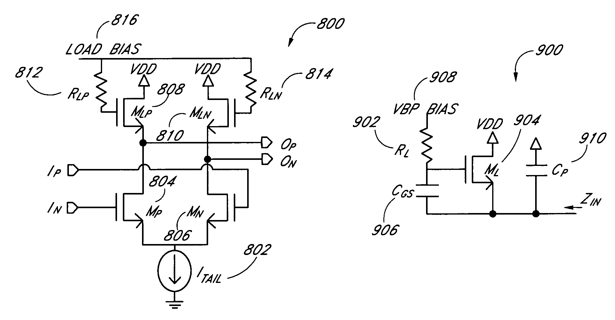
[0080]FIG. 8 illustrates one embodiment of a structure for an actively-peaked current mode logic buffer 800. This logic buffer 800 can be compared with the conventional devices described earlier in connection with FIG. 2 and FIG. 5. As with the conventional devices, a current source 802 drives a differential pair 804, 806. However, the actively-peaked current mode logic buffer 800 is loaded with NMOS transistors 808, 810 with resistors 812, 814 in series with the gates and a special bias 816 for the gates of the NMOS device loads. These NMOS loads 808, 810 are configured in a voltage follower mode that have particular benefits to a high-speed logic family.

[0081]These NMOS device loads 808, 810 can be combined to create many different logic structures. These logic structures include an “OR” gate, an “AND” gate, a Mux, and a D-type flip flop. These structures can be created using a combination of differential pairs with the NMOS voltage follower load.

[0082]The...


PUM


Abstract

A method and apparatus for creating high speed logic circuits in a CMOS environment using current steering logic cells with actively-peaked NMOS or PMOS loads and the biasing of these logic cells is disclosed. The logic cells can include, for example, buffers, AND gates, OR gates, flip-flops, and latches. The current steering cells with actively-peaked loads can provide benefits such as reduced power consumption, smaller area, and higher speed performance over conventional devices. This performance boost is preferably achieved using NMOS followers with resistively degenerated gates to create frequency peaked transfer function of current-mode logic cells. These logic cells with actively-peaked loads can advantageously be used in circuits in which relatively good power area and performance are desired for state machine logic, parallel to serial conversions, serial to parallel conversions, and the like.

Description


Claims


Application Information

Patent Timeline
Owner MICROSEMI STORAGE SOLUTIONS
Why Eureka
Try Eureka