Compact DMD-based optical module

a technology of optical modules and optical modules, applied in the field of compact dmd-based optical modules, can solve the problems of affecting the operation of free-space optical systems employing such components, affecting the operation of free-space optical systems, and being particularly susceptible to thermal stress, so as to improve the optical interface, reduce the risk of thermal stress, and be less sensitive to movement, vibration or mechanical stress.

Inactive Publication Date: 2007-04-10
TEXAS INSTR INC
View PDF46 Cites 11 Cited by
  • Summary
  • Abstract
  • Description
  • Claims
  • Application Information

AI Technical Summary

Benefits of technology

[0004]Disclosed herein is an improved optical interface system for a DMD array. The embodiments described herein provide for an improved optical interface system that is less sensitive to movement, vibration or mechanical stresses. The described embodiments further provide an optical interface system that occupies less space than conventional free-space optical interface systems. Also described herein is an optical interface system that can add optical functionality such as wavelength demultiplexing in close proximity to a DMD array in a compact footprint as a replacement to discrete free-space optical components. The above features are described in certain embodiments as incorporating all of the components of an optical interface system into a single, integral component.

Problems solved by technology

There are several difficulties that may be associated with the use of lenses, polarizers, mirrors and other such components in a free-space optical system.
Second, the operation of a free-space optical system employing such components can be affected by movement, vibration, or mechanical stress.
Third, free-space optical systems may be relatively large in size compared to other types of optical systems.
Fourth, given their relatively large size, free-space optical systems may be especially susceptible to thermal stresses; in particular, if one portion of the system is heated to a greater extent than the rest of the system, this can affect the alignment and performance of the entire system.

Method used


Image

  • Compact DMD-based optical module
  • Compact DMD-based optical module
  • Compact DMD-based optical module

Examples


Embodiment Construction

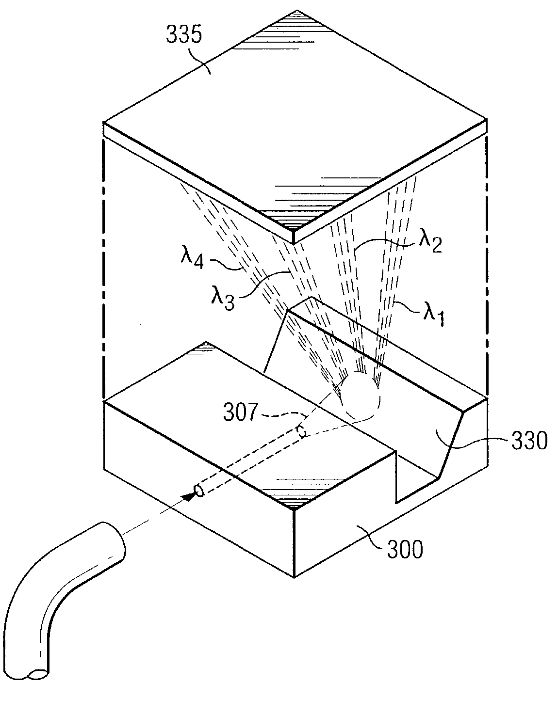
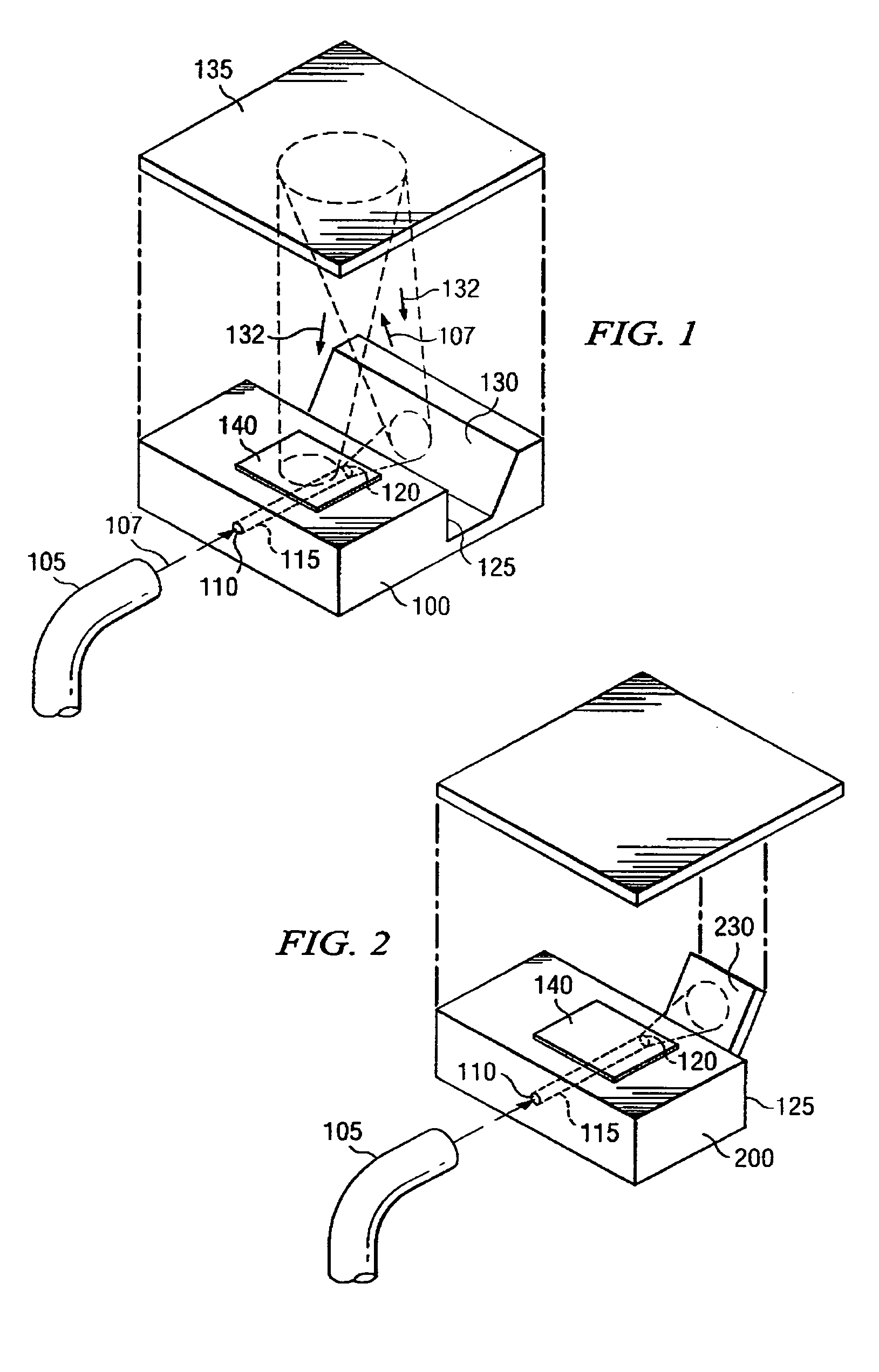
[0016]One embodiment of an improved optical interface system is depicted in FIG. 1. In FIG. 1, an optical module 100 is depicted as comprising a unitary piece that includes a waveguide 115 that passes from a first waveguide port 110 to a second waveguide port 120, which is located on an inside face 125 of the module 100. The optical module 100 may comprise a variety of materials, including Silicon (Si), Silicon Dioxide (SiO2), III–V semiconductor materials (e.g., InP, GaAs, AlGaAs, or some other combination of one or more Group III elements with one or more Group V elements), and II-VI semiconductor materials (e.g., ZnSe, ZnMgSSe, or some other of one or more Group II elements with one or more Group VI elements). The optical module 100 also comprises a reflective surface 130 that can reflect light emitted from the second waveguide port 120 onto a DMD array 135. The reflective surface 130 may comprise a variety of surfaces and substances that reflect light, including, for example, a ...


PUM


Abstract

An optical module having an integral optical waveguide with waveguide ports at each end. The optical waveguide receives an input light beam through a first waveguide port. The input light beam passes through the waveguide and is emitted from the second waveguide port, where it is reflected by the reflective surface. After being reflected by the reflective surface, the input light beam can be directed onto the surface of a DMD array, where the input light beam can be selectively reflected in a particular direction. The reflective surface may also comprise a diffractive grating, thereby enabling wavelength selective switching. In addition, the reflective surface may comprise a generally concave surface that converts a diverging input light beam into a generally collimated light beam, thereby facilitating more accurate selection and switching by the DMD array.

Description

BACKGROUND[0001]Micromechanical devices are small structures typically fabricated on a semiconductor wafer using techniques such as optical lithography, metal sputtering, oxide deposition, and etching that have been developed for the fabrication of integrated circuits. Digital micromirror devices (DMDs), sometimes referred to as deformable mirror devices, are a type of micromechanical device. Digital micromirror devices can be used in a variety of applications such as optical display systems or optical switching systems.[0002]DMD arrays have many advantages when used in optical switching systems. Specifically, a DMD array has the ability to selectively reflect portions of a light beam that is directed onto its surface. This feature can be used to implement a variety of functions such as signal monitoring, or wavelength-based switching. U.S. Pat. No. 6,295,154 entitled “Optical Switching Apparatus,” which is hereby incorporated by reference, describes the use of DMD arrays for these ...

Claims


Application Information

Patent Timeline
Patent Type & Authority Patents(United States)
IPC IPC(8): G02B6/34G02B6/26G02B6/42G02B6/35
CPCG02B6/352G02B6/3552G02B6/356G02B6/3588G02B6/3594G02B6/4214
Inventor KOONTZ, ELISABETH MARLEYPOWELL, DONALD A.
Owner TEXAS INSTR INC
Why Eureka
Try Eureka