Double-sided display device and method of fabricating the same

a display device and display device technology, applied in the direction of luminescnet screens, identification means, instruments, etc., can solve the problems of deteriorating display performance, difficult connection operation, and display device not meeting the requirement of reducing size, so as to achieve the effect of reducing spa

Inactive Publication Date: 2007-05-01
TOHOKU PIONEER CORP
View PDF2 Cites 27 Cited by
  • Summary
  • Abstract
  • Description
  • Claims
  • Application Information

AI Technical Summary

Benefits of technology

[0009]The present invention has an object of coping with the above-described problems. Specifically, in a double-sided display device including: a pair of substrates, each including a self-emitting element area formed thereon, the substrates being bonded to each other so that their faces carrying the self-emitting element areas face each other; and display planes, each being formed on the side of a bottom face of each of the substrates, the display planes being formed so as to be oriented in opposite directions, the present invention has objects of allowing easy connection of lead wiring sections formed on the respective ends of the substrates with a driving circuit component, a wiring substrate, or the like, and enabling the reduction in space where a panel of the double-sided display device is placed or where the entire module including the driving circuit component, the wiring substrate, or the like is placed.

Problems solved by technology

In the case of the organic EL display device, a sealing structure for blocking organic EL elements formed on a substrate from the outside air is required because the organic EL elements have a property of deteriorating its display performance when they are exposed to the outside air containing moisture and the like.
Accordingly, there arises a problem that, when one of the lead wiring sections is connected to the driving circuit component, the wiring substrate, or the like, the other lead wiring section interferes in connection, making the connecting operation difficult.
Accordingly, there arises a problem that such a display device does not satisfy the requirement of reduction in size, which is requested for mounting it on small electronic equipment.
Therefore, an excessively large space in electronic equipment is occupied by the plurality of driving circuit components, wiring substrates or the like.
Also in this regard, there arises the problem that the requirement of reduction in size is not satisfied.

Method used


Image

  • Double-sided display device and method of fabricating the same
  • Double-sided display device and method of fabricating the same
  • Double-sided display device and method of fabricating the same

Examples


Embodiment Construction

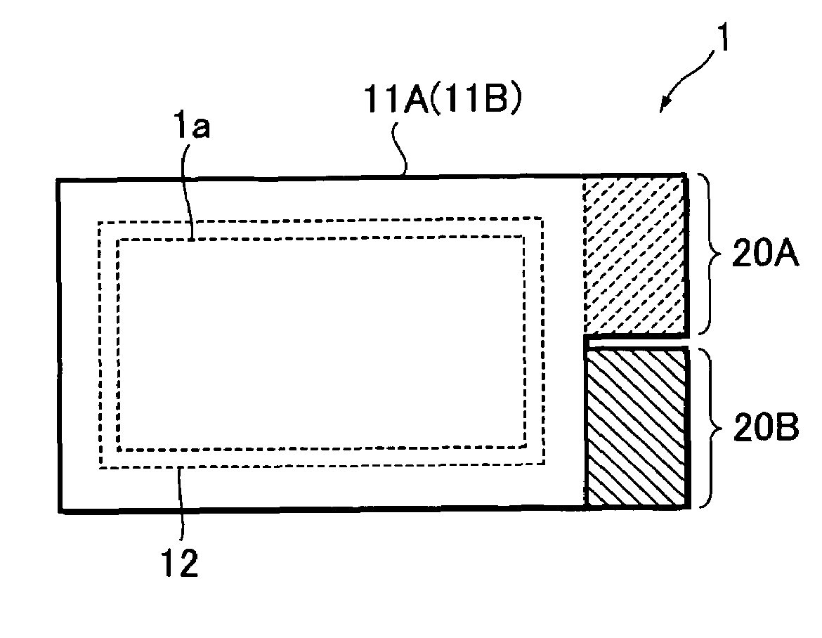
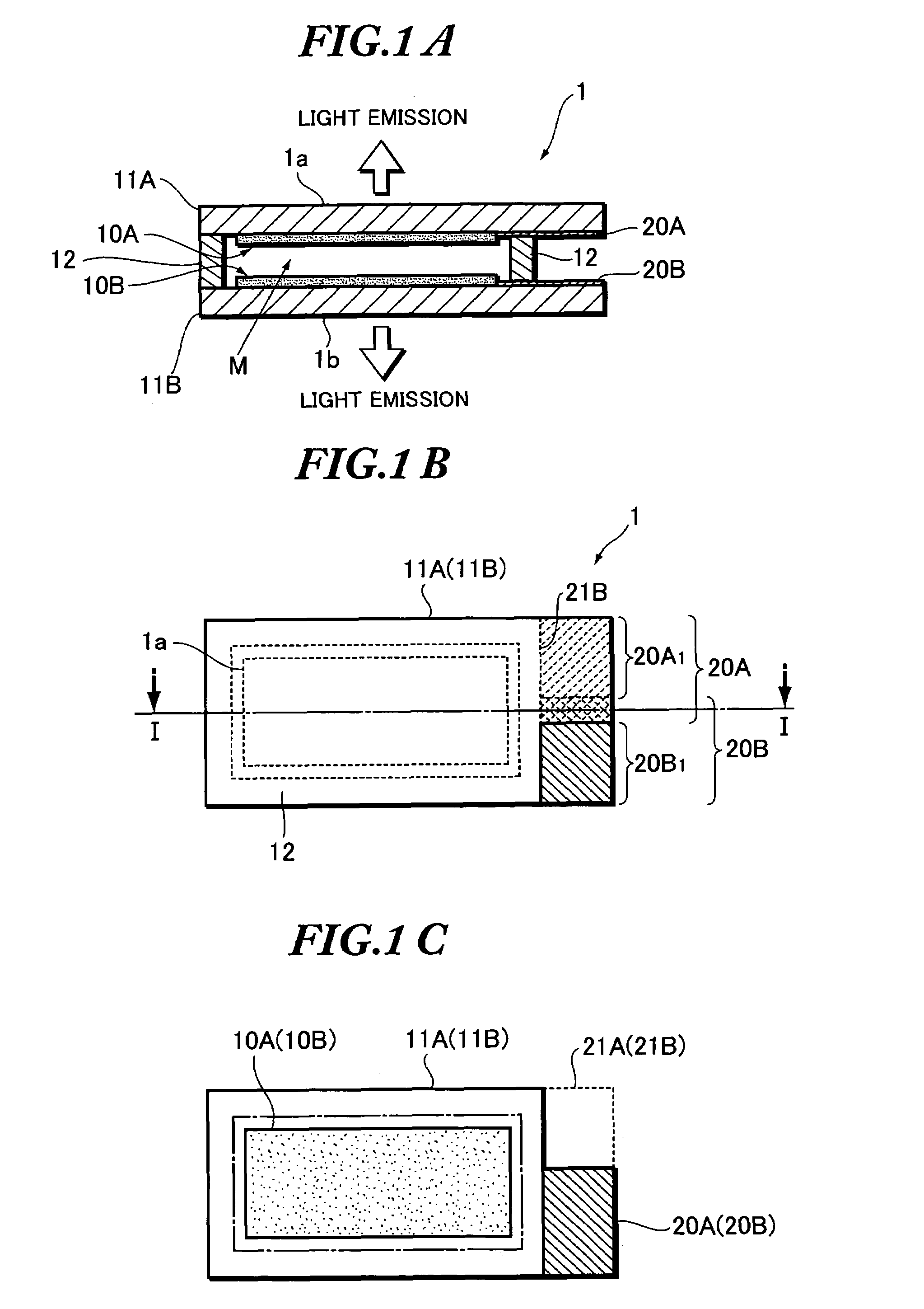
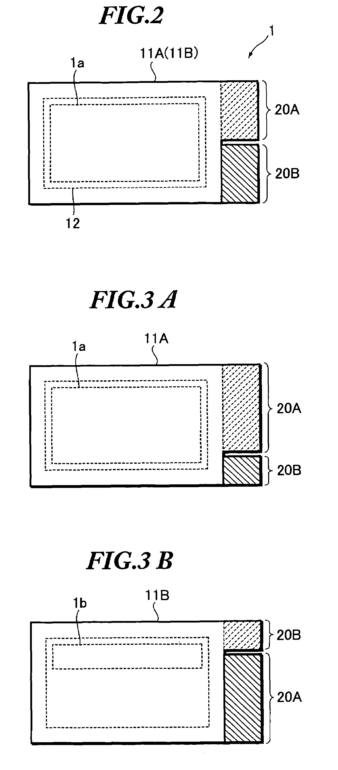
[0022]Hereinafter, an embodiment of the present invention will be described with reference to the accompanying drawings. FIGS. 1A to 1C are explanatory views showing a structure of a double-sided display device according to an embodiment of the present invention FIG. 1A is a sectional view taken along the line I—I in FIG. 1B, FIG. 1B is a plan view showing the double-sided display device, and FIG. 1C is a plan view when viewed from the side of one of substrates, on which a self-emitting element area is formed. A double-sided display device 1 has the following configuration. A pair of substrates 11A and 11B, on which self-emitting element areas 10A and 10B are respectively formed, are bonded to each other so that their faces carrying the self-emitting element areas 10A and 10B face each other. Display planes 1a and 1b are formed on the bottom face sides of the substrates 11A and 11B, respectively, so as to be oriented in opposite directions.

[0023]Each of the self-emitting element are...


PUM


Abstract

A double-sided display device includes a pair of substrates, on which self-emitting elements are formed respectively, being bonded to each other. A lead wiring section of the self-emitting element area formed on one of the substrates and a lead wiring section of the self-emitting element area formed on the other substrate are formed on the same side of the substrates. Each of the lead wiring sections is formed in a part of the side of each of the substrates. In addition, cutout portions are formed in parts of the sides of the substrates where the lead wiring sections are not formed. Thus, in the double-sided display device, the lead wiring sections formed on ends of substrates can be easily connected with a driving circuit component, a wiring substrate or the like, while the space for the double-sided display device can be reduced.

Description

BACKGROUND OF THE INVENTION[0001]The present invention relates to a double-sided display device and a method of fabricating the same.[0002]The present application claims priority from Japanese Patent Application No. 2004-067169, the disclosure of which is incorporated herein by reference.[0003]Various types of self-emitting flat panel display devices such as an organic electroluminescence (EL) display device, a plasma display panel (PDP), and a field emission display (FED) have recently been developed. In these display devices, a display is formed by arranging self-emitting elements on a substrate. Therefore, the display devices have attracted attention as display devices which are advantageous over liquid crystal displays requiring a backlight in possibility of reduction of power consumption as well as of thickness.[0004]Moreover, in the self-emitting flat panel display devices, substrates of two displays are bonded to each other so that their light-emitting sides are oriented outw...

Claims


Application Information

Patent Timeline
Patent Type & Authority Patents(United States)
IPC IPC(8): H01J61/94H05B33/06G09F9/00G09F9/30G09F9/40H01L27/32H01L51/50H05B33/10H05B33/12H05B33/26
CPCH01L27/3288H05B33/26H01L25/048H01L27/3267H01L27/3276H01L27/3286H01L2924/0002H01L2924/00H10K59/90H10K59/128H10K59/131H10K59/176H10K59/179
Inventor TANAKA, SHINSUKE
Owner TOHOKU PIONEER CORP
Why Eureka
Try Eureka