Semiconductor laser device

a laser device and semiconductor technology, applied in the field of semiconductor laser devices, can solve the problems of large change in emission wavelength, and achieve the effect of increasing wavelength and maximizing the gain of semiconductor laser devices

Inactive Publication Date: 2007-05-08
MITSUBISHI ELECTRIC CORP
View PDF19 Cites 0 Cited by
  • Summary
  • Abstract
  • Description
  • Claims
  • Application Information

AI Technical Summary

Benefits of technology

[0010]According to one aspect of the present invention, a semiconductor laser device comprises an active layer, a cladding layer, and an end face for emitting light. A low-reflective film is provided on the end face. The reflectance of the low-reflective film changes with wavelength. A wavelength at which the reflectance of the low-reflective film is minimized is on the long wavelength side of a wavelength at which the gain of the semiconductor laser device is maximized. The gain and the loss of the semiconductor laser device become equal at a wavelength only in a wavelength region in which the reflectance of the low-reflective film decreases with increasing wavelength.

Problems solved by technology

Furthermore, the conventional semiconductor laser device exhibits a large change in the emission wavelength due to the temperature dependence of its gain, which causes a significant problem when it is used for applications requiring a stable-wavelength light source.

Method used


Image

  • Semiconductor laser device
  • Semiconductor laser device
  • Semiconductor laser device

Examples


Embodiment Construction

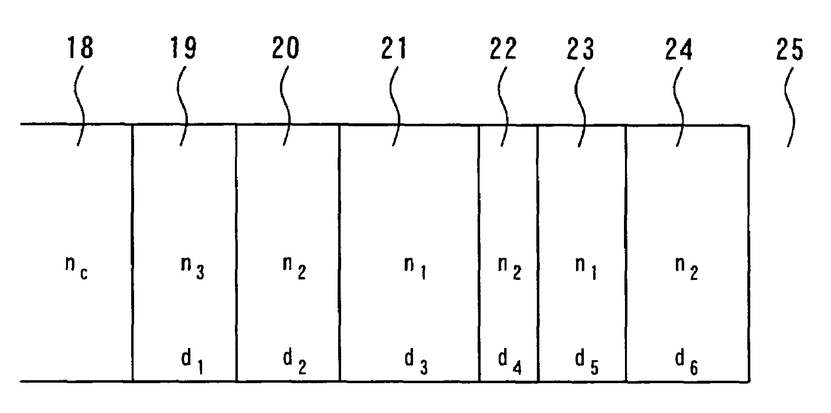
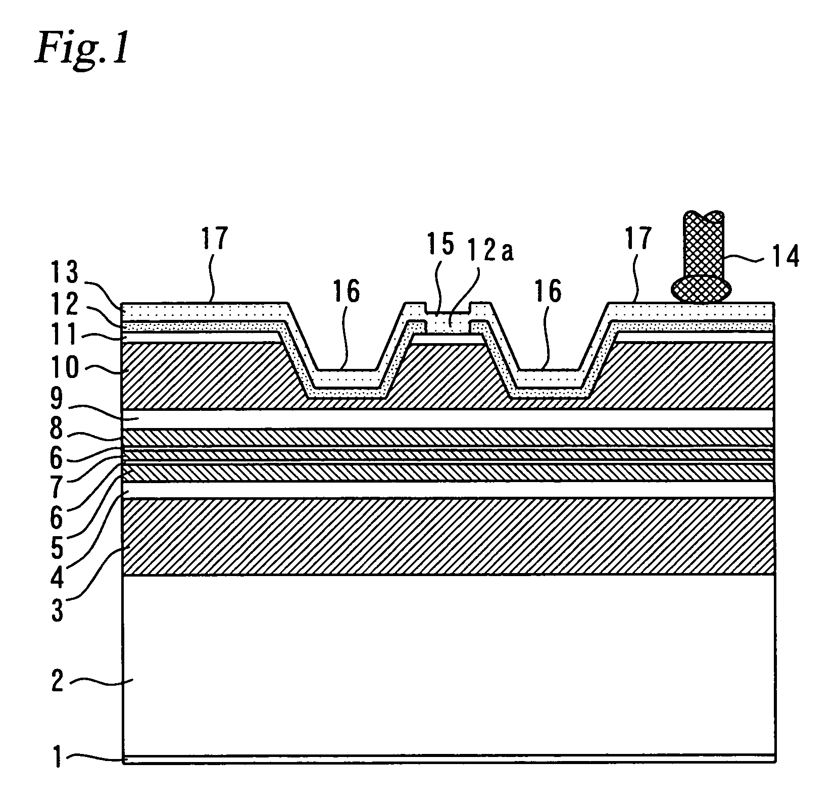
[0025]FIG. 1 shows a cross-sectional view of a semiconductor laser device according to an embodiment of the present invention. Referring to FIG. 1, reference numeral 1 denotes an n-side electrode; 2, an n-side GaAs substrate; 3, an n-side AlGaAs cladding layer; 4, an undoped n-side AlGaAs guide layer; 5, an undoped n-side GaAs guide layer; 6, an undoped InGaAs quantum well active layer; 7, an undoped GaAs barrier layer; 8, an undoped p-side GaAs guide layer; 9, an undoped p-side AlGaAs guide layer; 10, a p-side AlGaAs cladding layer; 11, a p-side GaAs capping layer; 12, an Si3N4 insulating film; 13, a p-side electrode; 14, a gold wire; 15, a ridge region; 16, low refractive index regions which sandwich the ridge region 15; and 17, high refractive index regions which sandwich the low refractive index regions 16. In the figure, the gold wire 14 is wire-bonded onto one of the high refractive index regions 17.

[0026]As shown in FIG. 1, the low refractive index regions 16 sandwich the rid...


PUM


Abstract

A semiconductor laser device comprises an active layer, a cladding layer, an end face for emitting light. A low-reflective film is provided on the end face. The reflectance of the low-reflective film changes with wavelength. A wavelength at which the reference of the low-reflective film is minimized is on the long wavelength side of a wavelength at which the gain of the semiconductor laser device is maximized. The gain and the loss of the semiconductor laser device become equal at a wavelength only in a wavelength region in which the reflectance of the low-reflective film decreases with increasing wavelength. The reflectance of the low-reflective film is preferably set to 1% or less at the wavelength at which the gain of the semiconductor laser device is maximized.

Description

BACKGROUND OF THE INVENTION[0001]1. Field of the Invention[0002]The present invention relates to a semiconductor laser device used as a light source for optical information processing, a signal source for optical communications, or an excitation light source for fiber amplifiers.[0003]2. Background Art[0004]FIG. 13 shows the relationship between the wavelength and the optical output power of a conventional semiconductor laser device. The semiconductor laser device of FIG. 13 is constructed such that an SiO2 film is provided on the front end face (emitting end face) and a multilayer film made up of SiO2 films and amorphous silicon films is provided on the rear end face. In this case, the reflectance of the front end face is 6% while that of the rear end face is 94% (see, for example, “High-power visible GaAlAs lasers with self-aligned stripe buried heterostructure”, by T. Ohtoshi et al., Journal of Applied Physics (US), 1984, vol. 56, No. 9, pp. 2491–2496).[0005]Referring to FIG. 13,...

Claims


Application Information

Patent Timeline
Patent Type & Authority Patents(United States)
IPC IPC(8): H01S5/00H01S5/028H01S5/22H01S5/223H01S5/30H01S5/343
CPCB82Y20/00H01S5/028H01S5/2231H01S5/0287H01S5/2214H01S5/34313H01S5/30
Inventor SHIGIHARA, KIMIOKAWASAKI, KAZUSHIGE
Owner MITSUBISHI ELECTRIC CORP
Why Eureka
Try Eureka