Large area self imaging lithography based on broadband light source

a self-imagery, broadband technology, applied in the field of lithography, can solve problems such as inability to achieve width-based features

Active Publication Date: 2020-06-25
APPLIED MATERIALS INC
View PDF0 Cites 0 Cited by
  • Summary
  • Abstract
  • Description
  • Claims
  • Application Information

AI Technical Summary

Benefits of technology

[0005]In another embodiment, a method is provided. The method includes projecting an initial light beam of a plurality of light beams at a minimum wavelength to a mask in a propagation direction of the plurality of light beams. The mask has a plurality of dispersive elements. A wavelength of each light beam of the plurality of light beams is increased until a final light beam of the plurality of light beams is projected at a maximum wavelength. The plurality of dispersive elements of the mask diffract the plurality of light beams into order mode beams to produce an intensity pattern in a medium between the mask and a substrate having a photoresist layer disposed thereon. The intensity pattern having a plurality of intensity peaks writes a plurality of portions in the photoresist layer.
[0006]In yet another embodiment, a method is provided. The method includes projecting a plurality of light beams concurrently to a mask in a propagation direction of the plurality of light beams. Each light beam of the plurality of light beams has a different wavelength not less than a minimum wavelength and not greater than a maximum wavelength of a plurality of wavelengths. A plurality of dispersive elements of the mask diffract the plurality of light beams into order mode beams to produce an intensity pattern in a medium between the mask and a substrate having a photoresist layer disposed thereon. The intensity pattern having a plurality of intensity peaks writes a plurality of portions in the photoresist layer.

Problems solved by technology

However, there are demands and device trends for features having widths not obtainable by conventional lithographic processes.

Method used


Image

  • Large area self imaging lithography based on broadband light source
  • Large area self imaging lithography based on broadband light source
  • Large area self imaging lithography based on broadband light source

Examples


Embodiment Construction

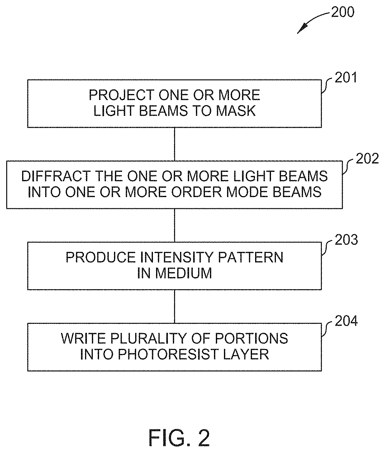
[0021]Embodiments described herein provide a method of large area lithography to decrease widths of portions written into photoresists. One embodiment of the method includes projecting an initial light beam of a plurality of light beams at a minimum wavelength to a mask in a propagation direction of the plurality of light beams. The mask has a plurality of dispersive elements. A wavelength of each light beam of the plurality of light beams is increased until a final light beam of the plurality of light beams is projected at a maximum wavelength. The plurality of dispersive elements of the mask diffract the plurality of light beams into order mode beams to produce an intensity pattern in a medium between the mask and a substrate having a photoresist layer disposed thereon. The intensity pattern having a plurality of intensity peaks writes a plurality of portions in the photoresist layer.

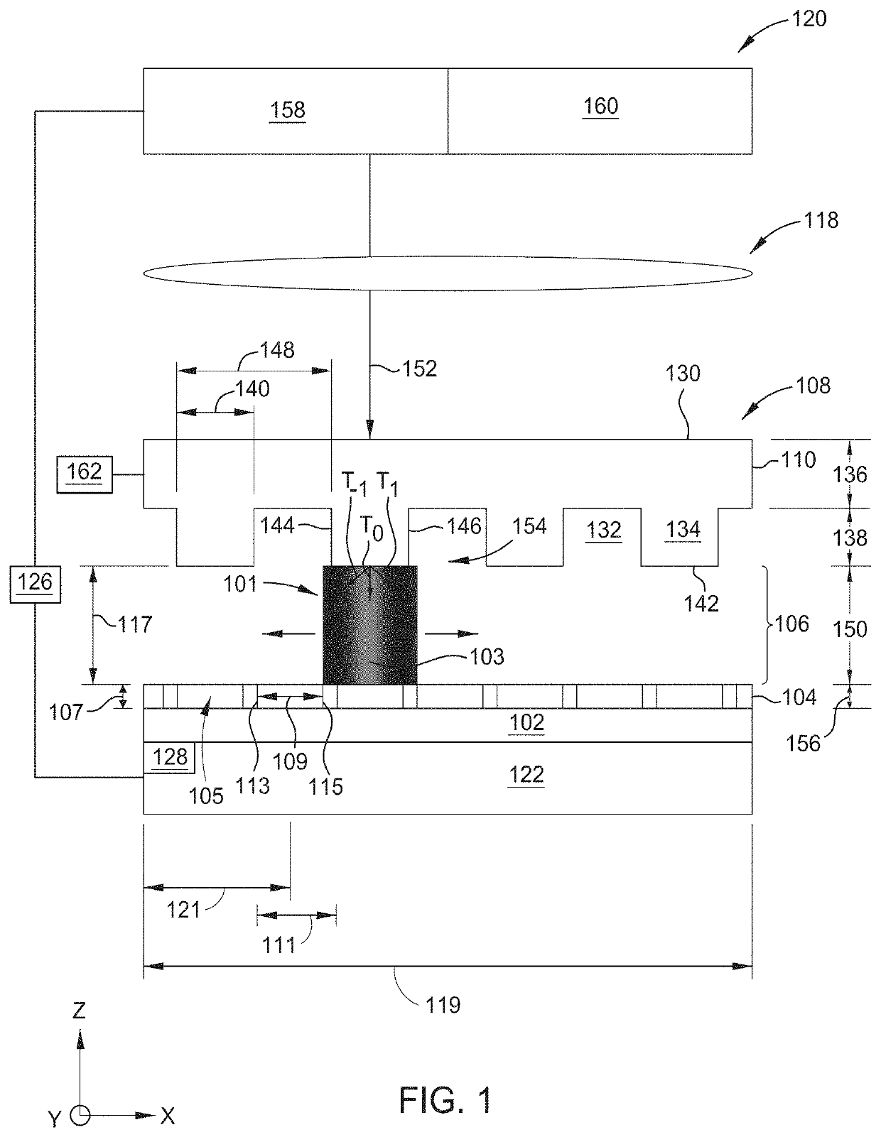
[0022]FIG. 1 is a schematic view of a system 100, such as a lithography system, that may benefit f...


PUM

PropertyMeasurementUnit
central wavelengthaaaaaaaaaa
refractive indexaaaaaaaaaa
central wavelengthaaaaaaaaaa

Abstract

Embodiments described herein provide a method of large area lithography to decrease widths of portions written into photoresists. One embodiment of the method includes projecting an initial light beam of a plurality of light beams at a minimum wavelength to a mask in a propagation direction of the plurality of light beams. The mask has a plurality of dispersive elements. A wavelength of each light beam of the plurality of light beams is increased until a final light beam of the plurality of light beams is projected at a maximum wavelength. The plurality of dispersive elements of the mask diffract the plurality of light beams into order mode beams to produce an intensity pattern in a medium between the mask and a substrate having a photoresist layer disposed thereon. The intensity pattern having a plurality of intensity peaks writes a plurality of portions in the photoresist layer.

Description

BACKGROUNDField[0001]Embodiments of the present disclosure generally relate to lithography. More particularly, embodiments of the present disclosure relate to a method of large area lithography.Description of the Related Art[0002]Lithography is widely used in the manufacturing of optical components and waveguide structures used in display devices, such as flat panel displays. Large area substrates are often utilized in the manufacture flat panel displays. In one example, flat panel displays are commonly used for active matrix displays, such as computers, touch panel devices, personal digital assistants (PDAs), cell phones, television monitors, and the like.[0003]Conventional lithography of large area substrates includes projecting light beams to a mask. The mask receives the light beams and diffracts the light beams to produce an intensity pattern. Peaks of the intensity pattern write a plurality of portions having sub-micro widths into a photoresist disposed over a substrate positi...

Claims


Application Information

Patent Timeline
Patent Type & Authority Applications(United States)
IPC IPC(8): G03F7/20
CPCG03F7/70191G03F7/2006G03F7/70408G03F7/7005G03F7/0002G03F7/70058
Inventor CHADHA, ARVINDERCUNNINGHAM, KEVIN LAUGHTON
Owner APPLIED MATERIALS INC
Why Eureka
Try Eureka