Optoelectronic device with three-dimensional semiconductor elements

a technology of optoelectronic devices and semiconductor elements, applied in semiconductor devices, basic electric elements, electric devices, etc., can solve the problems of significant decrease in the quantum efficiency of the active area of the optoelectronic device, and achieve the effect of increasing the wavelength of electromagnetic radiation

Active Publication Date: 2020-04-07
COMMISSARIAT A LENERGIE ATOMIQUE ET AUX ENERGIES ALTERNATIVES +1
View PDF9 Cites 0 Cited by
  • Summary
  • Abstract
  • Description
  • Claims
  • Application Information

AI Technical Summary

Benefits of technology

[0012]Another object of an embodiment is to increase the wavelength of the electromagnetic radiation capable of being emitted or captured by the optoelectronic device.

Problems solved by technology

A disadvantage is that when the atomic percent of indium exceeds a threshold, lattice parameter differences can be observed between the GaN and InGaN of the quantum well, which may cause the forming of non-radiative defects in the active area, such as dislocations, which causes a significant decrease in the quantum efficiency of the active area of the optoelectronic device.

Method used


Image

  • Optoelectronic device with three-dimensional semiconductor elements
  • Optoelectronic device with three-dimensional semiconductor elements
  • Optoelectronic device with three-dimensional semiconductor elements

Examples


Embodiment Construction

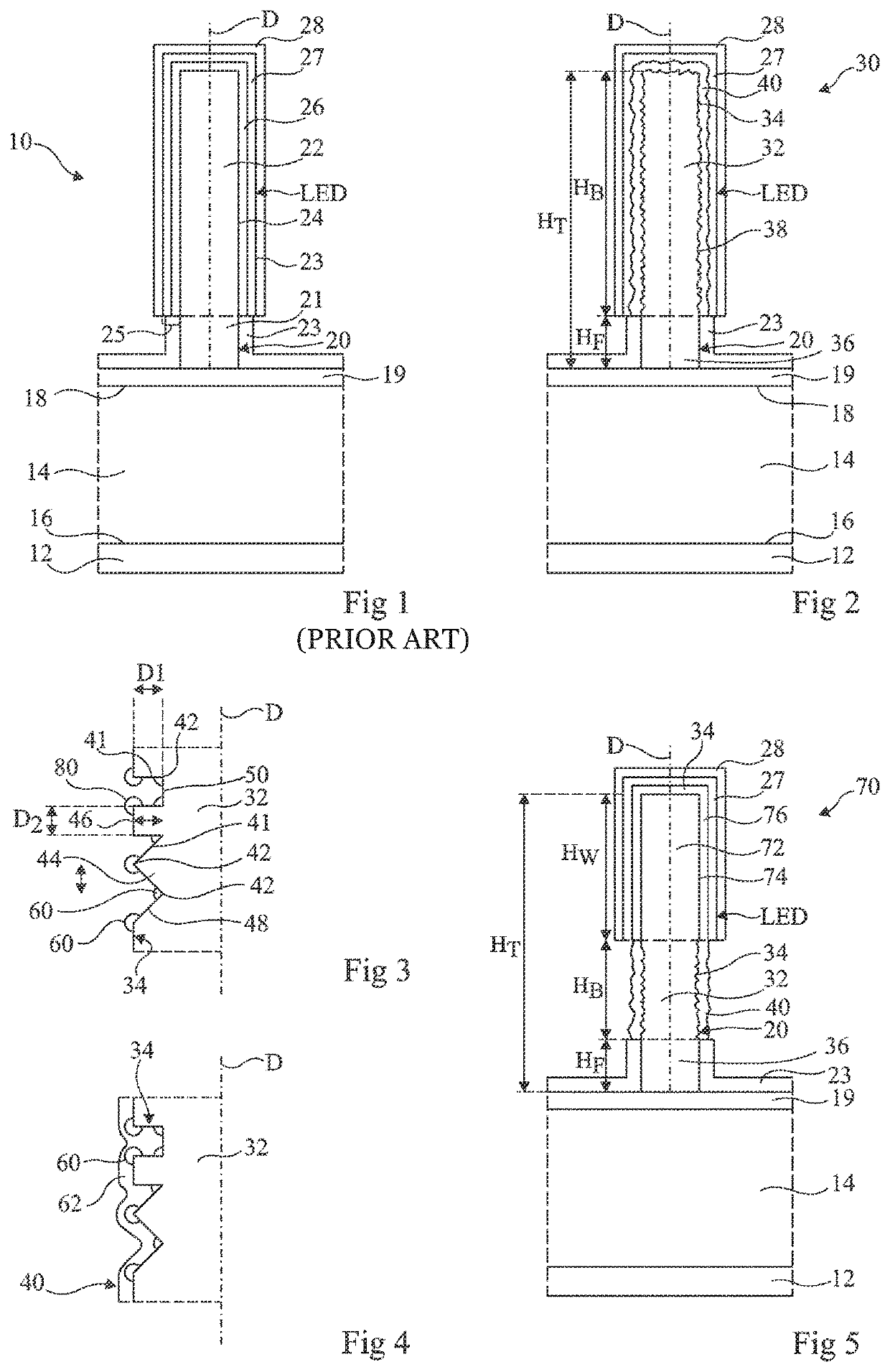
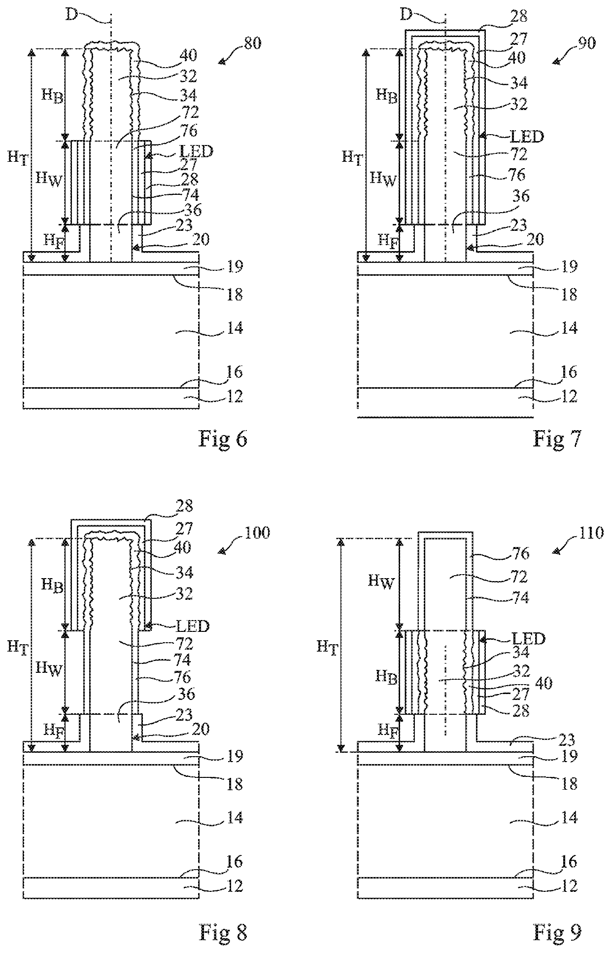
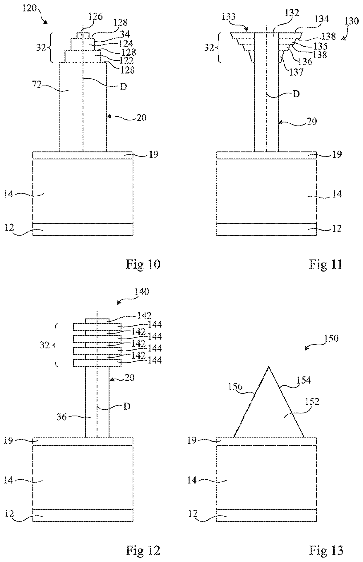
[0036]For clarity, the same elements have been designated with the same reference numerals in the various drawings and, further, as usual in the representation of electronic circuits, the various drawings are not to scale. Further, only those elements which are useful to the understanding of the present description have been shown and will be described. In particular, the means for controlling the optoelectronic device described hereafter are within the abilities of those skilled in the art and are not described. In the following description, unless otherwise indicated, terms “substantially”, “approximately”, and “in the order of” mean “to within 10%”.

[0037]The present description relates to optoelectronic devices comprising semiconductor elements having the shape of microwires, of nanowires, or of pyramids.

[0038]Term “microwire” or “nanowire” designates a three-dimensional structure having an elongated shape, for example, cylindrical, conical, or tapered, along a preferred directio...


PUM

PropertyMeasurementUnit
distanceaaaaaaaaaa
distanceaaaaaaaaaa
heightaaaaaaaaaa

Abstract

An optoelectronic device including three-dimensional semiconductor elements predominantly made of a first compound selected from among the group consisting of Compounds III-V, Compounds II-VI, and Compounds IV. Each semiconductor element defines, optionally with insulating portions partially covering said semiconductor element, at least one first surface including contiguous facets angled relative to each other. The optoelectronic device includes quantum dots at least some of the seams between the facets. The quantum dots are predominantly made of a mixture of the first compound and an additional element and are suitable for emitting or receiving a first electromagnetic radiation at a first wavelength.

Description

CROSS-REFERENCE TO RELATED APPLICATIONS[0001]This application is the national phase of International Application No. PCT / FR2015 / 052602, filed on Sep. 29, 2015, which claims priority to French Patent Application No. 14 / 59275, filed Sep. 30, 2014, each of which applications is incorporated herein by reference to the maximum extent allowable.[0002]The present patent application claims the priority benefit of French patent application FR14 / 59275 which will be incorporated herein by reference.BACKGROUND[0003]The present invention generally relates to optoelectronic devices made from semiconductor materials and to methods of manufacturing the same.[0004]Term “optoelectronic devices” is used to designate devices capable of converting an electric signal into an electromagnetic radiation or the other way, and especially devices dedicated to detecting, measuring, or emitting an electromagnetic radiation or devices dedicated to photovoltaic applications.DISCUSSION OF THE RELATED ART[0005]Radia...

Claims


Application Information

Patent Timeline
Patent Type & Authority Patents(United States)
IPC IPC(8): H01L33/00H01L33/24H01L31/0352H01L33/06H01L33/18H01L33/22
CPCH01L33/24H01L33/06H01L31/035209H01L33/18H01L33/22H01L33/0054H01L33/0062H01L33/04
Inventor ROBIN, IVAN-CHRISTOPHEDUSSAIGNE, AMÉLIEFEUILLET, GUYGAUGIRAN, STÉPHANIE
Owner COMMISSARIAT A LENERGIE ATOMIQUE ET AUX ENERGIES ALTERNATIVES
Why Eureka
Try Eureka