Electronic Display Device Having An Electroluminescent Screen and Its Fabrication Process

a technology of electroluminescent screen and electronic display device, which is applied in the manufacture of electrode systems, electric discharge tubes/lamps, and discharge tubes based on small molecules. it is impossible to microstructure small molecules with conventional microelectronic technology, and the aperture of each subpixel is increasing

Active Publication Date: 2011-05-26
COMMISSARIAT A LENERGIE ATOMIQUE ET AUX ENERGIES ALTERNATIVES
View PDF5 Cites 0 Cited by
  • Summary
  • Abstract
  • Description
  • Claims
  • Application Information

AI Technical Summary

Benefits of technology

[0008]One object of the present invention is to provide a monochromatic or polychromatic electronic display device that allows this need to be met and which thus alleviates the aforementioned drawback, this device comprising an electroluminescent emission face and, towards the interior of this face, a substrate coated with a matrix of pixels, each pixel consisting of an organic light-emitting structure intermediate between and in electrical contact with two electrodes, one near and the other far relative to the substrate respectively, an electrically insulating resin covering the substrate between the respective near electrodes of the pixels and furthermore extending onto a peripheral edge of each near electrode.
[0009]For this purpose, a device according to the invention is such that each pixel incorporates at least one auxiliary electrode which is transparent or semitransparent to this light, which is based on a metallic material having a work function identical or substantially identical to that of the near electrode and which extends inclinedly on the surface of this resin and facing said edge, from the near electrode towards the far electrode, so as to maximize the emission area of each pixel and to vary the thickness of the optical cavity formed between the near electrode of each pixel and the far electrode.
[0012]It is pointed out that each auxiliary electrode according to the invention, which thus extends from the base electrode of a pixel or subpixel prolonging it towards the exterior (i.e. towards the far electrode) in the manner of a ramp, allows the emissive area of this pixel or subpixel to be increased relative to that of a known pixel or subpixel, the aperture of which is delimited only by the resin, because the planar electrical conduction of this auxiliary electrode is greater than the transverse conduction of the organic layers of the emitting structure that surmounts it. The peripheral width of each auxiliary electrode, which may for example vary from a few tenths of a micron to a few microns, thus provides the corresponding pixel or subpixel with a light-emitting peripheral edge in addition to, and comparable to, the central part of the pixel or subpixel defined by the region of the near electrode not covered by the resin. This results in an increase in the actual light-emitting area of all the pixels of the display device and therefore in an aperture ratio that may be substantially higher for the latter device relative to that of the aforementioned known devices, which leads to a minimized current density for a given luminance and therefore an extended lifetime of the device according to the invention.
[0017]It is furthermore pointed out that each auxiliary electrode which is formed on the surface of the resin, by being transparent or semitransparent (especially in the visible range), allows the thickness of the optical cavity of the corresponding pixel or subpixel to be spatially varied, which cavity is formed by the two, near and far, electrodes, it being clarified that this thickness may be modulated by the local topology of the underlying resin. The result of this spatial variation in the thickness of the optical cavity is an advantageous variation in the spectral response of the latter, as will be explained below.
[0018]It should be pointed out that each auxiliary electrode has the advantage, because it is transparent or semitransparent and also because it marries precisely the gently sloping profile of the resin, of not altering the operation of this optical cavity, especially for filtered broad-spectrum white light-emitting structures.
[0020]This monotonic increasing variation (i.e. exclusively towards the far electrode) of each auxiliary electrode allows the wavelengths of the subpixels to be amplified in turn and allows the light spectrum emitted by all the pixels of the device to be broadened.

Problems solved by technology

Production of such microdisplay or microscreen devices, i.e. having pixels with side lengths of less than 50 μm, gives rise to many technical problems due to this targeted small pixel size and in particular to the use of OLED technology which, for each pixel, uses a light-emitting multilayer structure comprising an organic film intermediate between two, internal and external, electrodes that serve as anode and cathode, one of which is transparent or semitransparent to the emitted light whereas the other is generally reflective.
In fact, OLEDs based on small molecules cannot be microstructured with conventional microelectronic technologies and it is therefore impossible for three separate emitting structures, emitting in the red, the green and the blue respectively, to be spatially deposited on one and the same internal base electrode so as to form the three subpixels of each pixel.
However, one major drawback of this lithography is that the aperture of each subpixel (which increases as the coverage of the base electrode by the resin decreases) must be written in the unetched metal surface of this base electrode.

Method used


Image

  • Electronic Display Device Having An Electroluminescent Screen and Its Fabrication Process
  • Electronic Display Device Having An Electroluminescent Screen and Its Fabrication Process
  • Electronic Display Device Having An Electroluminescent Screen and Its Fabrication Process

Examples


Embodiment Construction

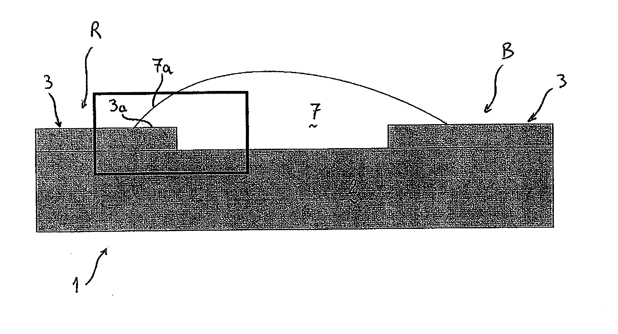
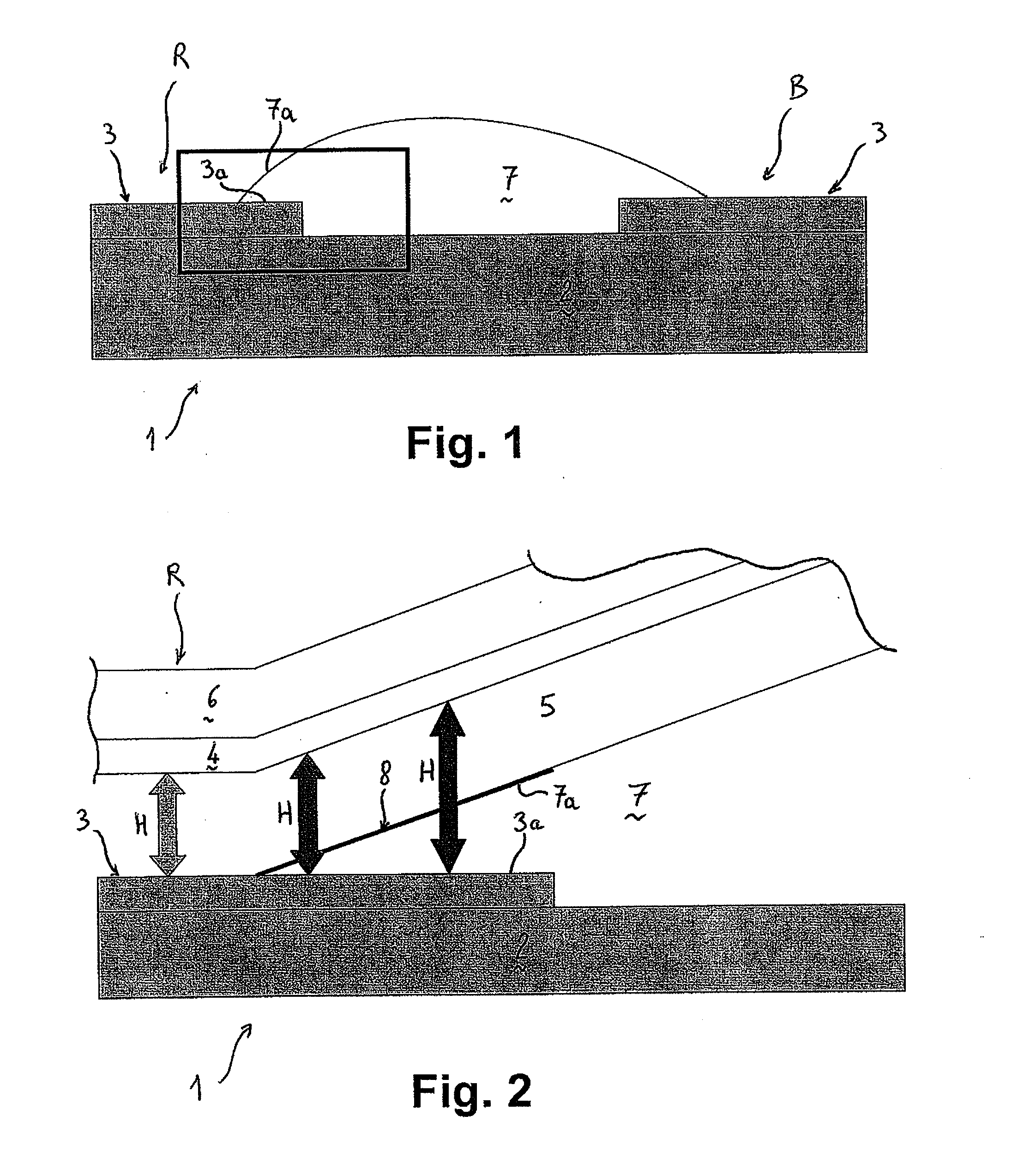
[0032]The following description of the invention given with reference to FIGS. 1 and 2 relates to a polychromatic microdisplay but it will be noted that it could equally apply to a monochromatic microdisplay on condition that the subpixels be replaced with pixels.

[0033]The polychromatic microdisplay 1 according to the invention during fabrication, schematized in FIGS. 1 and 2, is an OLED microdisplay and it comprises a substrate 2, for example made of silicon, coated with an active matrix of pixels, two adjacent subpixels, or colour dots, R and B of which are identified in FIG. 1, for each pixel, by their near base electrode 3, i.e. near relative to the substrate 2, which base electrode is chosen to be transparent or semitransparent and that plays the role, for example, of an anode. This array of base electrodes 3, defining the set of subpixels R, G, B of each pixel, surmounts, in a known way, an integrated circuit structure of the substrate 2 that serves to address each pixel and t...


PUM


Abstract

The invention relates to a electronic display device having an electroluminescent screen and to its manufacturing method.This device (1) comprises a substrate (2) coated with a matrix of pixels, each pixel formed by an organic emitting structure (5) intermediate between two electrodes, one (3) near and the other (4) far, relative to the substrate respectively, an electrically insulating resin (7) covering the substrate between the respective near electrodes of the pixels and furthermore extending onto a peripheral edge (3a) of each near electrode.According to the invention, each pixel incorporates at least one auxiliary electrode (8) which is transparent or semitransparent, which is based on a metallic material having a work function identical or substantially identical to that of the near electrode, and which extends inclinedly on the surface of the resin and facing said edge, from the near electrode towards the far electrode, so as to maximize the emission area of each pixel and to vary the thickness of the optical cavity formed between the near electrode of each pixel and the far electrode. This auxiliary electrode is implanted on the resin by dry etching of the material of the near electrode from which it is derived by ricochet.

Description

FIELD OF THE INVENTION[0001]The present invention relates to a monochromatic or polychromatic electronic display device having an electroluminescent screen and to its fabrication process. The invention applies in particular to active matrix microscreen or microdisplays surmounted by organic light-emitting diodes (OLEDs).BACKGROUND OF THE INVENTION[0002]In a known way, electroluminescent display devices comprise an emission region formed from a matrix of pixels, each pixel typically consisting of a plurality of differently coloured (RGB: red, green and blue, in general) subpixels, and from an electrical connection region arranged to lie adjacent this emission region. Production of such microdisplay or microscreen devices, i.e. having pixels with side lengths of less than 50 μm, gives rise to many technical problems due to this targeted small pixel size and in particular to the use of OLED technology which, for each pixel, uses a light-emitting multilayer structure comprising an organ...

Claims


Application Information

Patent Timeline
Patent Type & Authority Applications(United States)
IPC IPC(8): H01J1/62H01J9/00
CPCH01L27/3246H01L51/56H01L51/5203H01L51/0017H10K59/122H10K71/231H10K50/805H10K71/00H10K59/121
Inventor VAUFREY, DAVIDFLAHAUT, THIERRY
Owner COMMISSARIAT A LENERGIE ATOMIQUE ET AUX ENERGIES ALTERNATIVES
Why Eureka
Try Eureka