Semiconductor pressure sensor and method of producing the same

a pressure sensor and semiconductor technology, applied in semiconductor devices, instruments, measurement devices, etc., can solve the problems of recesses being moved with respect, likely to vary in thickness of diaphragm, etc., and achieve the effect of less variation in thickness, reduced thickness of diaphragm, and high accuracy

Inactive Publication Date: 2011-04-19
MITSUBISHI ELECTRIC CORP
View PDF15 Cites 7 Cited by
  • Summary
  • Abstract
  • Description
  • Claims
  • Application Information

AI Technical Summary

Benefits of technology

[0011]By the method of producing a semiconductor pressure sensor according to the present invention, predetermined films formed on the front surface of the substrate constitute the diaphragm. Accordingly, the diaphragm can be reduced in thickness with high accuracy only by changing the predetermined films in thickness. Further, by forming an opening in the insulation film and forming the anchor portion in the opening, the region surrounded by the anchor portion is specified as a region to constitute the diaphragm. This ensures that the gauge resistor provided for the diaphragm can be located with accuracy. The region of diaphragm as well as the position of gauge resistor and the like can therefore be controlled by processing the first main surface of the substrate. Consequently, the diaphragm of reduced and less varied thickness can be formed with accuracy in the predetermined region, while size reduction of the semiconductor pressure sensor can be achieved.

Problems solved by technology

However, conventional semiconductor pressure sensors have the following drawbacks.
Accordingly, the diaphragm is controlled in thickness by the etching time, causing the problem in that the diaphragm is likely to vary in thickness in the region to constitute the diaphragm.
There is another problem in that variations in the amount of etching of the silicon substrate cause the recesses to be displaced with respect to the gauge resistors provided for the diaphragm.

Method used


Image

  • Semiconductor pressure sensor and method of producing the same
  • Semiconductor pressure sensor and method of producing the same
  • Semiconductor pressure sensor and method of producing the same

Examples


first embodiment

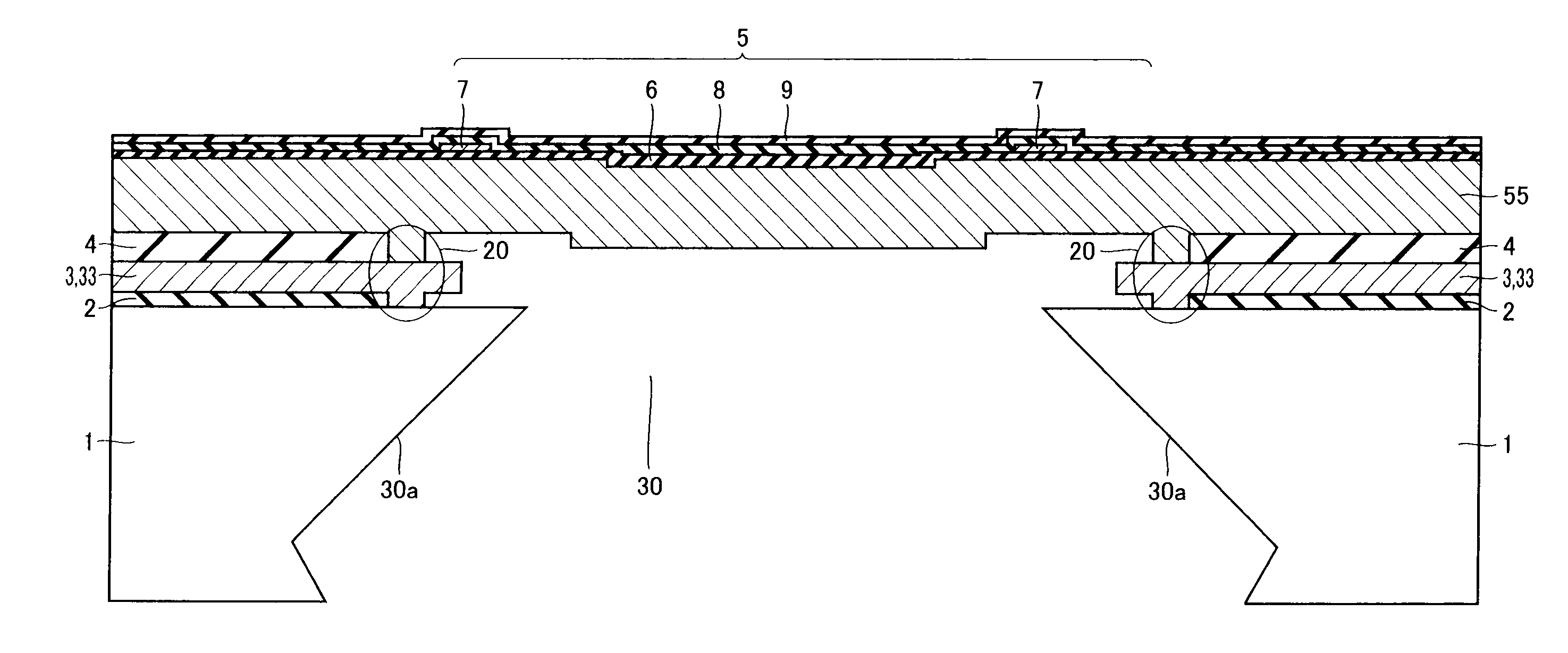
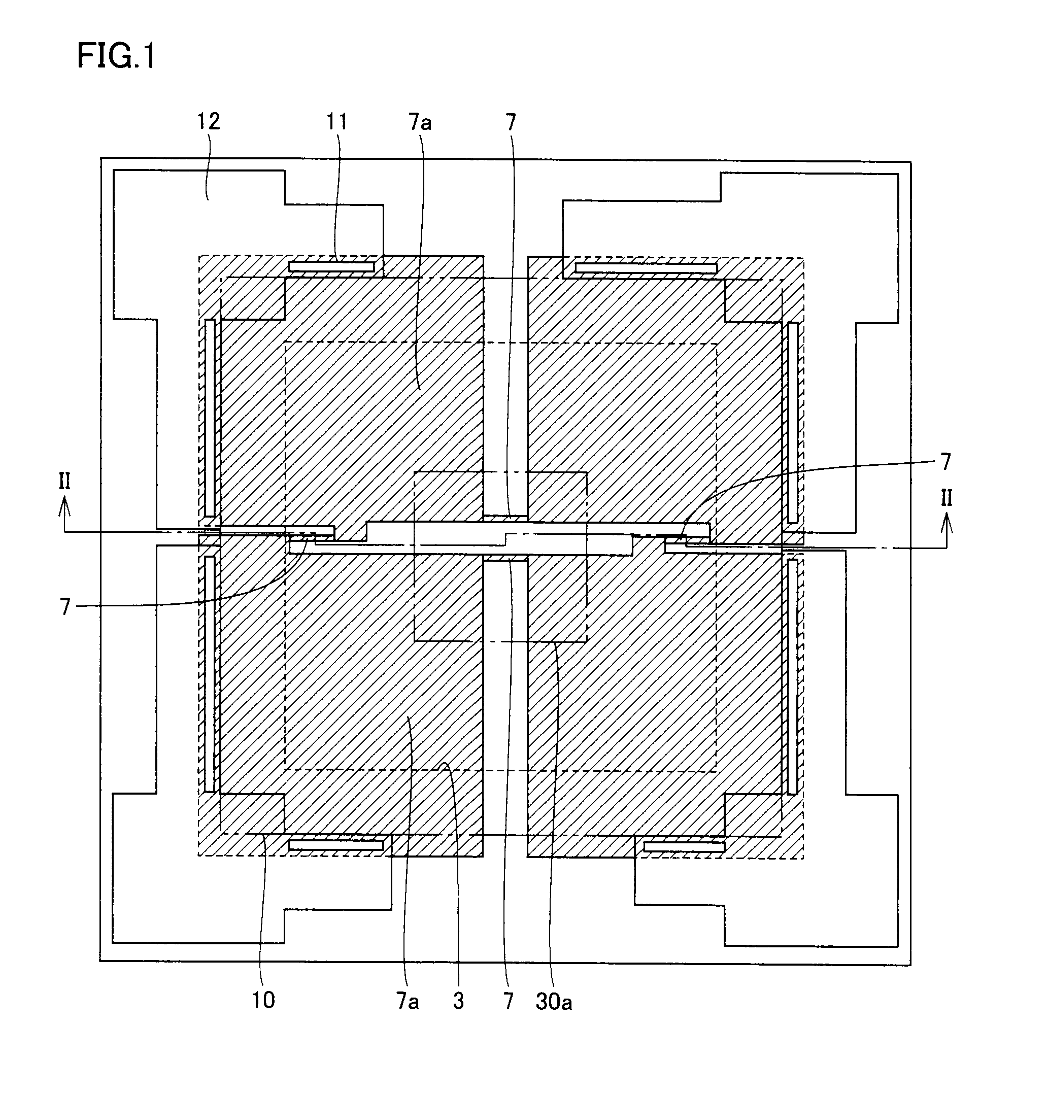
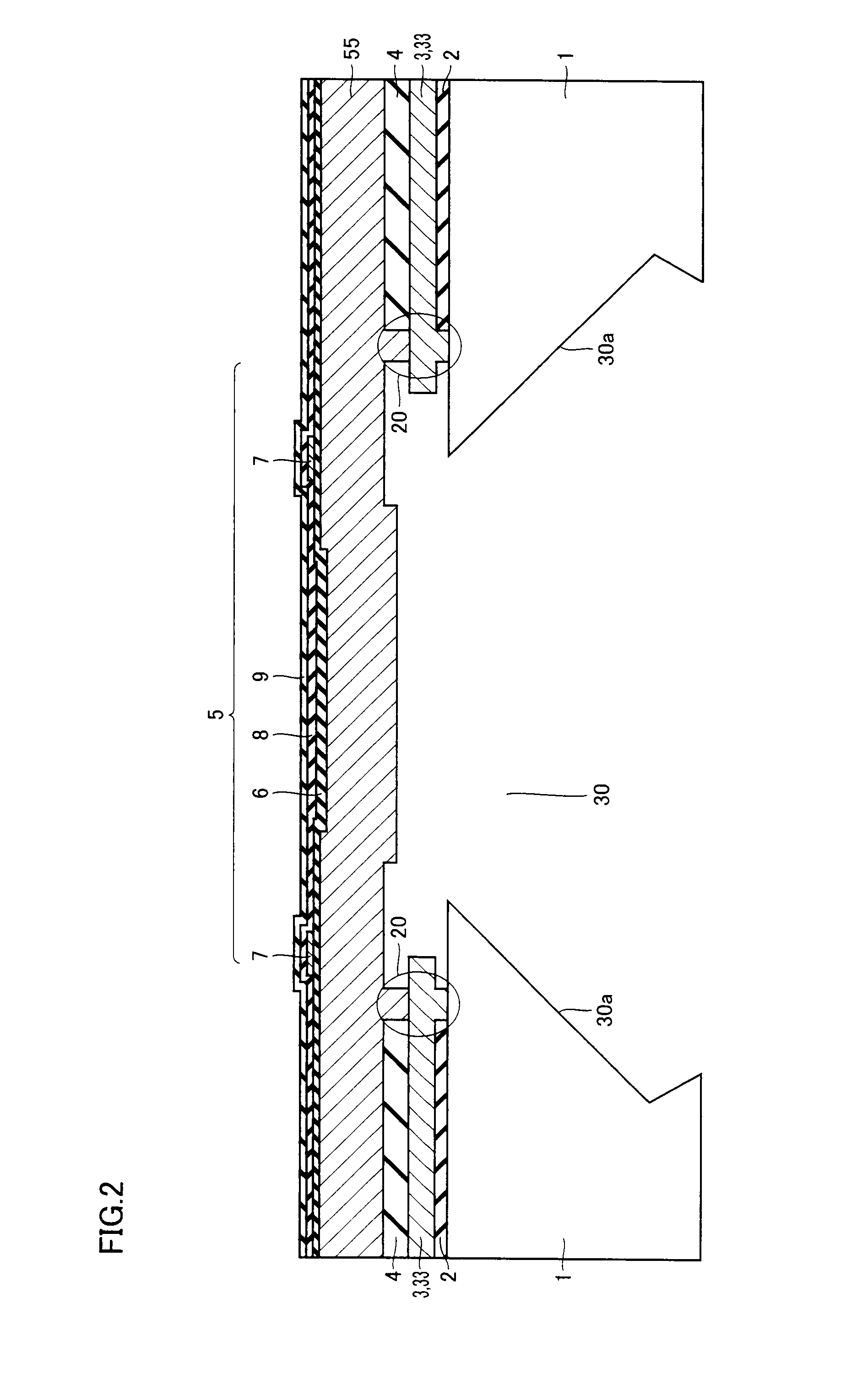
[0043]A semiconductor pressure sensor having gauge resistors on the top face of a diaphragm made of a doped polysilicon film will now be described.

[0044]As shown in FIGS. 1 and 2, a silicon substrate 1 has formed above its first main surface a diaphragm 5 made of a doped polysilicon film 55. Diaphragm 5 has formed on its top face four gauge resistors 7 for sensing strain in diaphragm 5 as variations in electric resistance. A through hole 30 for exposing the bottom face of diaphragm 5 is formed in a portion of silicon substrate 1 above which diaphragm 5 is located. An anchor portion 20 for mounting diaphragm 5 on silicon substrate 1 is formed between diaphragm 5 and silicon substrate 1 in a manner surrounding circumferentially an opening end of through hole 30 located at the side facing the first main surface.

[0045]A first insulation film 2, a polysilicon sacrificial film 3 and a second insulation film 4 are stacked between diaphragm 5 and silicon substrate 1. Anchor portion 20 inclu...

second embodiment

[0062]A semiconductor pressure sensor having gauge resistors on each of the top and bottom faces of a diaphragm made of a doped polysilicon film will now be described.

[0063]As shown in FIGS. 9, 10 and 11, silicon substrate 1 has formed above its first main surface diaphragm 5 made of polysilicon film 55. Diaphragm 5 has two gauge resistors 7 provided on its top face and two gauge resistors 13 provided on its bottom face below gauge resistors 7. The region where gauge resistors 7 and 13 are located is surrounded by an isolation oxide film 14 extending through polysilicon film 55 to constitute diaphragm 5.

[0064]As shown in FIG. 12, two gauge resistors 77a and 77d located on the top face of diaphragm 5 and two gauge resistors 77b and 77c located on the bottom face are bridged. More specifically, gauge resistors 77a and 77b are connected electrically through the portion of doped polysilicon film 55 surrounded by isolation oxide film 14. Similarly, gauge resistors 77d and 77c are connect...

third embodiment

[0079]A semiconductor pressure sensor having a dummy polysilicon pattern will now be described. As shown in FIG. 17, in the present semiconductor pressure sensor, a dummy polysilicon pattern 7b having a width corresponding to that of gauge resistors 7 is provided along with the pattern of gauge resistors 7. Dummy polysilicon pattern 7b and gauge resistors 7 have a width of about 0.6 to 1.0 μm. Polysilicon interconnection 7a has a width of about 2 to 200 μm. The remaining structure is similar to that of the semiconductor pressure sensor shown in FIG. 1 and the like, like components are denoted by like reference characters, and description thereof will not be repeated.

[0080]To increase the piezoresistance coefficient of gauge resistors made of a polysilicon film, it is desirable to reduce the area in cross section. Reducing the gauge resistors in width will cause a resist (pattern) to be likely to vary in width in photolithography. This may cause variations in the final width of the g...


PUM

PropertyMeasurementUnit
thicknessaaaaaaaaaa
pressureaaaaaaaaaa
thicknessaaaaaaaaaa

Abstract

A diaphragm made of a polysilicon film is provided above a first main surface of a silicon substrate. Four gauge resistors are provided on the top face of the diaphragm. A through hole for exposing the bottom face of the diaphragm is formed in the silicon substrate. An anchor portion for mounting the diaphragm on the silicon substrate is provided between the diaphragm and the silicon substrate in a manner surrounding circumferentially an opening end of the through hole located at the side facing the first main surface. Accordingly, a semiconductor pressure sensor having a diaphragm of reduced and less varied thickness can be obtained.

Description

BACKGROUND OF THE INVENTION[0001]1. Field of the Invention[0002]The present invention relates to a semiconductor pressure sensor and a method of producing the same, and more particularly relates to a semiconductor pressure sensor having bridged gauge resistors and a method of producing such a semiconductor pressure sensor.[0003]2. Description of the Background Art[0004]One form of pressure sensors is a semiconductor pressure sensor to which a semiconductor substrate is applied. This semiconductor pressure sensor includes a plurality of diffused resistors to constitute gauge resistors, formed on the surface of a silicon substrate. These diffused resistors are bridged by diffused wiring layers having a low resistance. For example, the gauge resistors are located respectively on the four sides of a predetermined region to constitute a rectangular diaphragm. The silicon substrate has formed on its back surface recesses depressed toward the predetermined region of the front surface. This...

Claims


Application Information

Patent Timeline
Patent Type & Authority Patents(United States)
IPC IPC(8): G01L9/06
CPCG01L9/0055G01L9/0042G01L9/00G01L9/04H01L29/84
Inventor SATO, KIMITOSHI
Owner MITSUBISHI ELECTRIC CORP
Why Eureka
Try Eureka