Integrated circuit package employing a heat-spreader member

a technology of integrated circuits and heatspreaders, which is applied in the direction of cooling/ventilation/heating modifications, semiconductor device details, semiconductor/solid-state device details, etc., can solve the problems of increased package thickness, increased risk of overheating, and increased footprint of the package, so as to reduce the footprint of the integrated circuit, reduce the penalty, and reduce the effect of heat generation within the stack

Inactive Publication Date: 2007-05-29
INFINEON TECH AG
View PDF19 Cites 12 Cited by
  • Summary
  • Abstract
  • Description
  • Claims
  • Application Information

AI Technical Summary

Benefits of technology

[0012]Thus, the invention makes it possible to provide an integrated circuit package including a substrate and a plurality of stacked integrated circuits. Since the stacked integrated circuits project through the aperture in the substrate, the thickness of the package in the region of the integrated circuits does not depend upon the thickness of the substrate. Thus, the advantages of a stacked package (reduced integrated circuit footprint compared to a side-by-side arrangement) can be achieved with a reduced penalty in terms of the thickness of the package.
[0013]Furthermore, the heat-spreader member may be in intimate contact with at least one integrated circuit of the stack, and thus is highly effective in dissipating heat generated within the stack.
[0020]The heat-spreader member may optionally be attached (e.g., adhered) to this flat surface, so improve the heat conduction to it. The surface may, for example, be a motherboard.
[0021]Since the integrated circuits are mounted in the aperture in the substrate, the thickness of the package in the region of the integrated circuits does not depend upon the thickness of the flexible substrate. Thus, the advantages of a stacked package (reduced integrated circuit footprint compared to a side-by-side arrangement) can be achieved with a reduced penalty in terms of the thickness of the package.

Problems solved by technology

One disadvantage with providing a stacked die package assembly is that the thickness of the package is increased.
Additionally, there are reliability concerns due to the reduced possibilities for heat dissipation, which in turn lead to an increased risk of overheating.
Conversely, providing the dies side-by-side means that the footprint of the package is increased.

Method used


Image

  • Integrated circuit package employing a heat-spreader member
  • Integrated circuit package employing a heat-spreader member
  • Integrated circuit package employing a heat-spreader member

Examples


Embodiment Construction

[0027]The making and using of the presently preferred embodiments are discussed in detail below. It should be appreciated, however, that the present invention provides many applicable inventive concepts that can be embodied in a wide variety of specific contexts. The specific embodiments discussed are merely illustrative of specific ways to make and use the invention, and do not limit the scope of the invention.

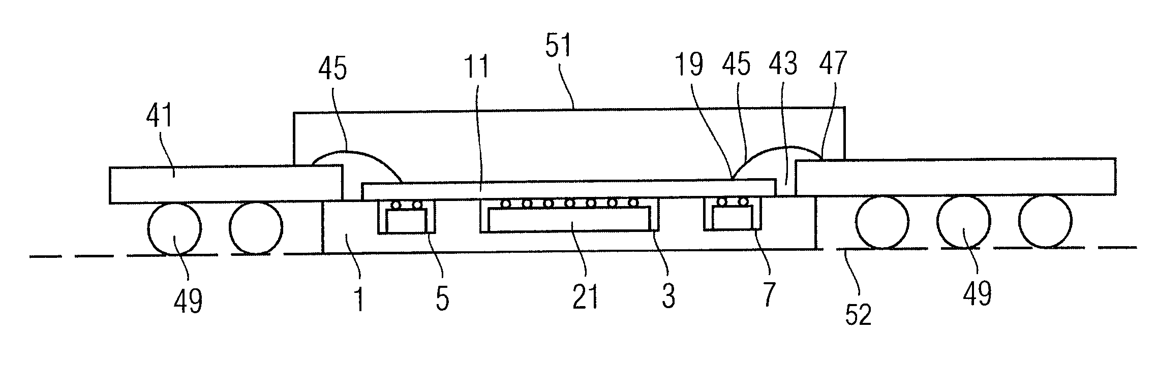
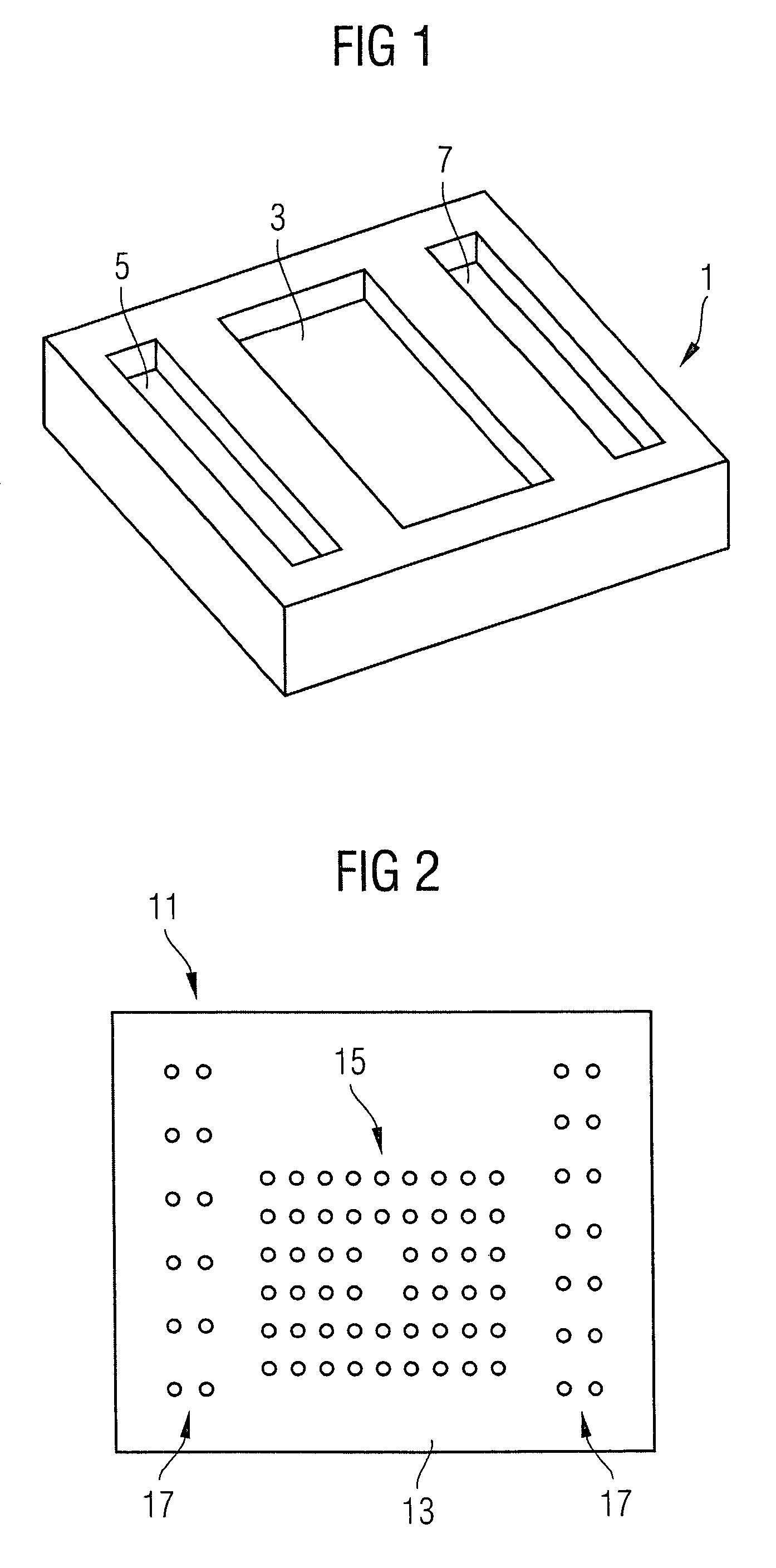
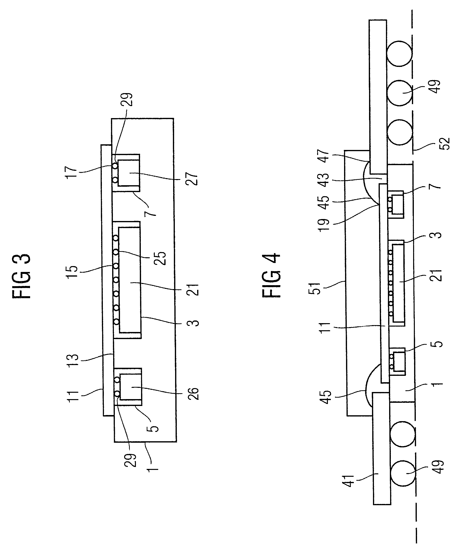
[0028]Referring firstly to FIG. 1, a heat-spreader member 1 is shown in a perspective view. The member is generally cuboidal, having two major surfaces of which one is shown directed upwardly. This major surface includes three cavities 3, 5, 7, which may be of the same depth or of different depths. The material of the heat-spreader member 1 may be made of a thermally conductive material, such as aluminum or copper.

[0029]Turning to FIG. 2, a first integrated circuit11 is shown looking toward one of its major surfaces 13. The surface 13 includes first electrical contacts 15, an...


PUM


Abstract

An integrated circuit package is proposed in which a laminar substrate 41 is provided with an aperture 43. A heat-spreader member 1 is mounted to cover this aperture 43, and contains a cavity 3 opening towards the aperture 43 in the substrate 41. A stack of integrated circuit circuits 11, 21, are located with one integrated circuit 21 of the stack inserted into the cavity 3, and one integrated circuit 11 of the stack electrically connected to the substrate 41.

Description

[0001]This application is a continuation of co-pending International Application No. PCT / SG2003 / 000126, filed May 28, 2003, which designated the United States and was published in English, and which application is incorporated herein by reference.TECHNICAL FIELD[0002]The present invention relates to methods of packaging integrated circuits using a heat-spreader member, and to integrated circuit packages produced using the method.BACKGROUND[0003]It is well known to provide integrated circuit packages in which integrated circuits (dies), principally composed of semiconductor material, are located within resin bodies. Electrical contacts of each integrated circuit are electrically in contact with corresponding electrical conductors, which protrude out of the resin body.[0004]In one type of package, the integrated circuits are located on a die pad portion of a lead frame with the electric contacts facing away from the lead frame, and wires are formed between the electric contacts and re...

Claims


Application Information

Patent Timeline
Patent Type & Authority Patents(United States)
IPC IPC(8): H01L23/34H01L21/00H05K7/20H01L23/13H01L23/31H01L23/433H01L25/065
CPCH01L23/13H01L23/3128H01L23/4334H01L25/0652H01L2224/48227H01L2924/01079H01L2924/15153H01L2924/15165H01L2924/19041H01L24/48H01L2924/01322H01L24/45H01L2224/05599H01L2224/45144H01L2224/85399H01L2924/00014H01L2924/14H01L2924/181H01L2224/45015H01L2924/207H01L2924/00H01L2924/00012
Inventor FERNANDEZ, ELSTAN ANTHONY
Owner INFINEON TECH AG
Why Eureka
Try Eureka