Circuit wiring layout in semiconductor memory device and layout method

a semiconductor memory and circuit wiring technology, applied in semiconductor/solid-state device details, digital storage, tension measurement, etc., can solve the problems of more difficult to form similarly sized transistors, write operation errors may occur, write operation errors may be caused, etc., to reduce the area occupied by peripheral circuit regions adjoining, and smoothly perform circuit wiring layout, the effect of reducing the resistive line loading of column decoding signal lines

Inactive Publication Date: 2009-07-21
SAMSUNG ELECTRONICS CO LTD
View PDF3 Cites 116 Cited by
  • Summary
  • Abstract
  • Description
  • Claims
  • Application Information

AI Technical Summary

Benefits of technology

[0027]An exemplary embodiment of the invention provides a circuit layout structure and layout method for a semiconductor memory device, which is capable of reducing the area occupied by a peripheral circuit region adjoining a memory cell region.
[0028]Another exemplary embodiment of the invention provides a circuit wiring layout structure capable of smoothly performing a wiring layout of circuit at a peripheral circuit region adjacent to a memory cell region of a semiconductor memory device, and of solving one write speed limiting factor.
[0029]Another exemplary embodiment of the invention provides a circuit layout structure and method in a semiconductor memory device, which is capable of substantially reducing a resistive line loading of column decoding signal lines in a column (Y) gating block, thereby preventing a write error. Further, transistors constituting a row decoder section, and wiring layers necessary for the operation of the row decoder section, can be configured appropriately to match the cell pitch of high-integrated memory cell. Transistors constituting a column (Y) gating block, and transistors constituting a row decoder section, can be disposed more efficiently in a limited size, and wiring layers necessary for the operation of the transistors can be formed to correspond to the reduced cell pitch of memory cells high-integrated in two or three dimensions, in a volatile semiconductor memory device.

Problems solved by technology

Regardless of the disposition of transistors constituting the memory cell on the same layer or mutually different layers, when the cell pitch of a memory cell is reduced, it is more difficult to form similarly sized transistors constituting the precharge and equalization part and the read and write path switching part.
Since parasitic resistances PR1, PR2, PR11 and PR22 may have very large values, errors in write operation may occur.
And thus, a write operation error may be caused.
In the case where wiring lines transmitting the column decoding signals Y0 and Y1 have a relatively large resistance component, the write operation is not performed smoothly.
Herewith, in the case that a silicide process is not well performed, a (sheet) resistance value of the wiring line may amount to several decades to hundreds of ohms.
A more serious variation of critical dimension for a gate poly makes a silicide process not well performed (not smooth).
If the silicide process is performed unstably, a wiring line transmitting a signal such as the column (Y) decoding signal has a large resistance-loading, thus may cause error in a write operation.
In other words, in a conventional technology referred to in FIGS. 4A and 4B a column fail rate may increase with a great reduction of manufacturing yield.

Method used


Image

  • Circuit wiring layout in semiconductor memory device and layout method
  • Circuit wiring layout in semiconductor memory device and layout method
  • Circuit wiring layout in semiconductor memory device and layout method

Examples


Embodiment Construction

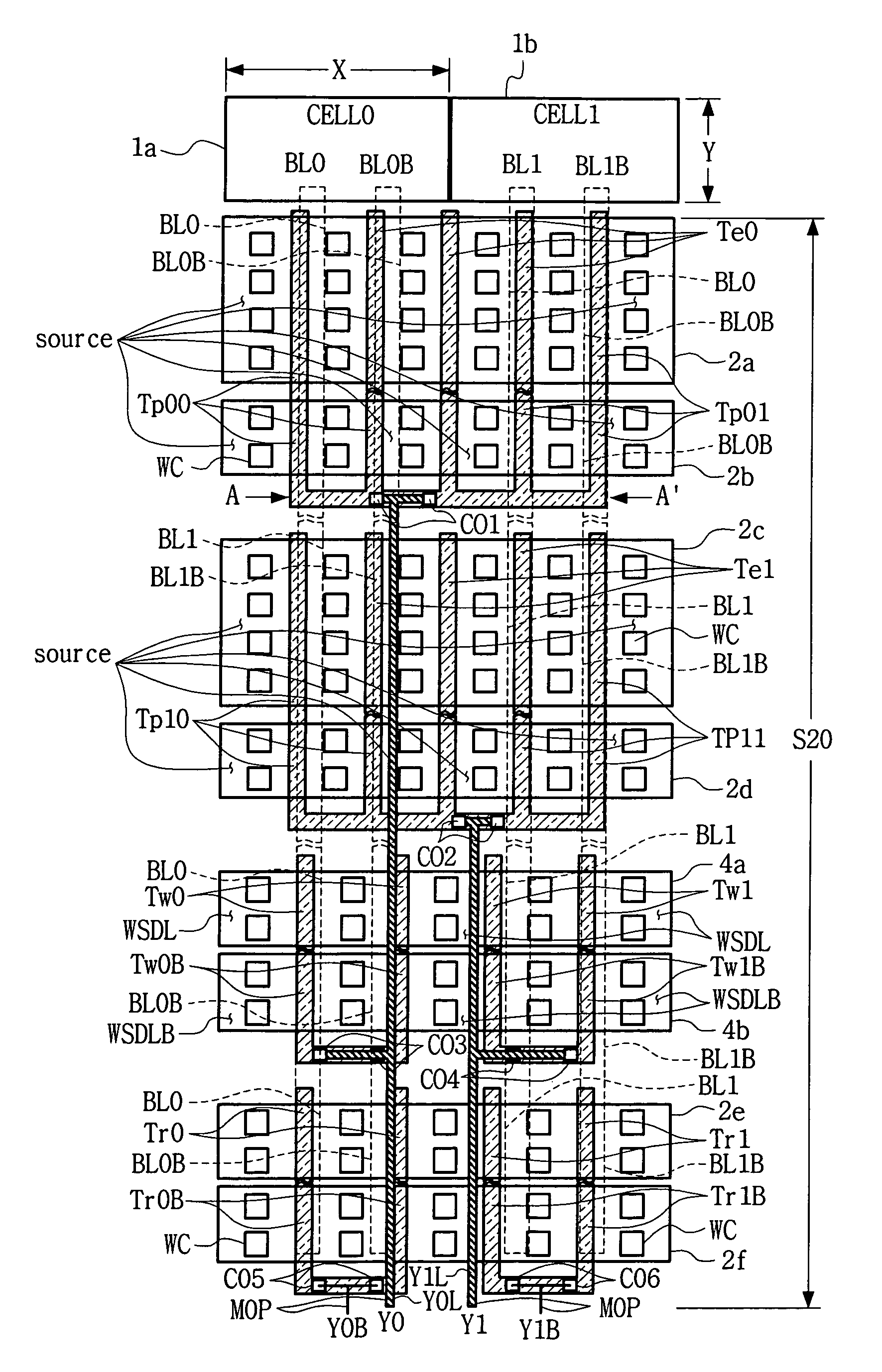
[0047]A first exemplary embodiment of the invention is shown in FIG. 6.

[0048]FIG. 6 is a plan view for a layout of the circuit shown in FIG. 2 according to an exemplary embodiment of the invention. The overall size (dimension S20) of second dimension (Y direction) is about 17 microns. The wiring lines transmitting column (Y) decoding signals are not formed by a silicide process. The layout structure shown in FIG. 6 may be applied to a device having memory cells having a vertical structure as shown in 5B (part of FIG. 5). The vertical structure of a memory cell region in a highly-integrated memory cell may vary between 5a and 5b shown in FIG. 5. It is beneficial to use a metal zero prime layer MOP (as any optional wire in a peripheral circuit region).

[0049]Referring to FIG. 5, in the conventional SRAM (see FIG. 3), an active layer L10 is connected to a metal zero layer M0;L15 through a tungsten contact L13, and the metal zero layer L15 is connected to a first metal layer L19 through ...


PUM

PropertyMeasurementUnit
sizeaaaaaaaaaa
sheet) resistanceaaaaaaaaaa
sizeaaaaaaaaaa

Abstract

An improved circuit wiring layout provides smooth circuit wiring in a peripheral circuit region adjacent to a memory cell region of a semiconductor memory device, and eliminates a write-speed limiting factor. Forming a metal (instead of a metal silicided polysilicon) wiring layer to be connected to a gate layer, to transmit an electrical signal to the gates of FET (e.g., MOSFET (Metal Oxide Semiconductor Field Effect Transistor) transistors formed in the peripheral circuit region; the metal wiring layer is formed (e.g., using one metal damascene process), on a layer different from a word line layer formed on the gate layer (e.g., using another metal damascene process), thereby obtaining a layout of a peripheral circuit region having a reduced area and without using a silicide process.

Description

[0001]The present invention relates to a semiconductor memory, and more particularly, to a circuit layout in a SRAM semiconductor memory device.BACKGROUND[0002]Very large scale integration, (VLSI), has allowed the electronics industry to reduce cost while continuing to increase chip performance and chip reliability. The performance of SRAM (Static Random Access Memory) chips may also be increased by reducing the device dimensions.[0003]Volatile semiconductor memory devices such as SRAMs are achieving higher speed and integration (miniaturization), corresponding to a growing demand for higher performance electronic systems such as personal computers or electronic communication equipments (e.g., cell phones, PDAs, etc.). Manufacturers of memory chips are making great efforts to improve the layout and manufacture of memory cells and peripheral circuits (which select and read the memory cells, such as sense amplifiers) connected with the memory cells, by reducing their dimensions. A cir...

Claims


Application Information

Patent Timeline
Patent Type & Authority Patents(United States)
IPC IPC(8): H01L23/48G01L5/06H01L23/52H01L29/40
CPCG11C5/063G11C11/417H01L27/11H01L27/1104Y10S257/903H01L2924/0002H01L2924/00H10B10/00H10B10/12H01L27/04
Inventor YANG, HYANG-JALEE, SONG-JA
Owner SAMSUNG ELECTRONICS CO LTD
Why Eureka
Try Eureka