Electrical bias electrical test apparatus and method

a technology of electrical test apparatus and bias, applied in the direction of individual semiconductor device testing, electric discharge tubes, instruments, etc., can solve the problems of difficulty in accurately and efficiently electrically testing microelectronic products, and achieve the effect of accurately and efficiently electrically testing and testing

a technology of electrical test apparatus and bias, applied in the direction of individual semiconductor device testing, electric discharge tubes, instruments, etc., can solve the problems of difficulty in accurately and efficiently electrically testing microelectronic products, and achieve the effect of accurately and efficiently electrically testing and testing

US7224173B2Inactive Publication Date: 2007-05-29TAIWAN SEMICON MFG CO LTD

Image

  • Electrical bias electrical test apparatus and method
  • Electrical bias electrical test apparatus and method
  • Electrical bias electrical test apparatus and method

Examples


Embodiment Construction

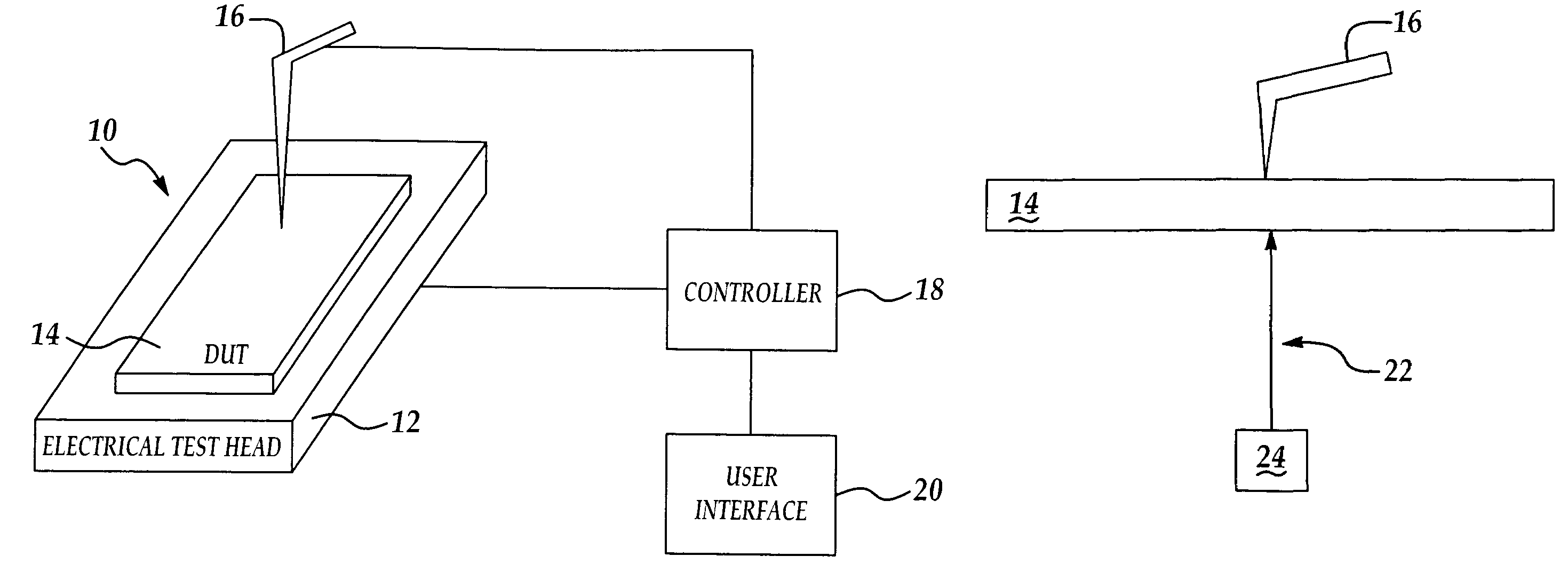
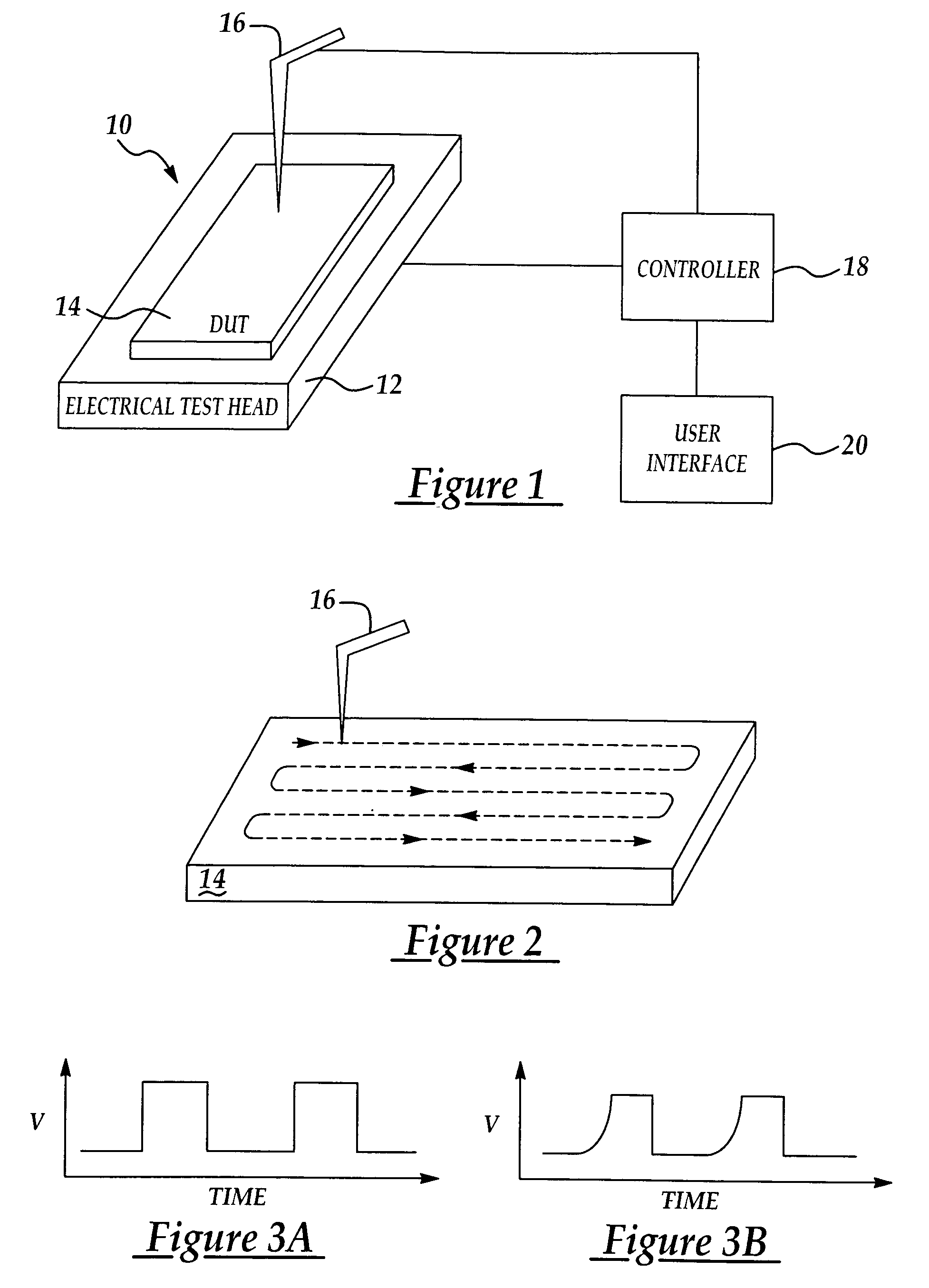
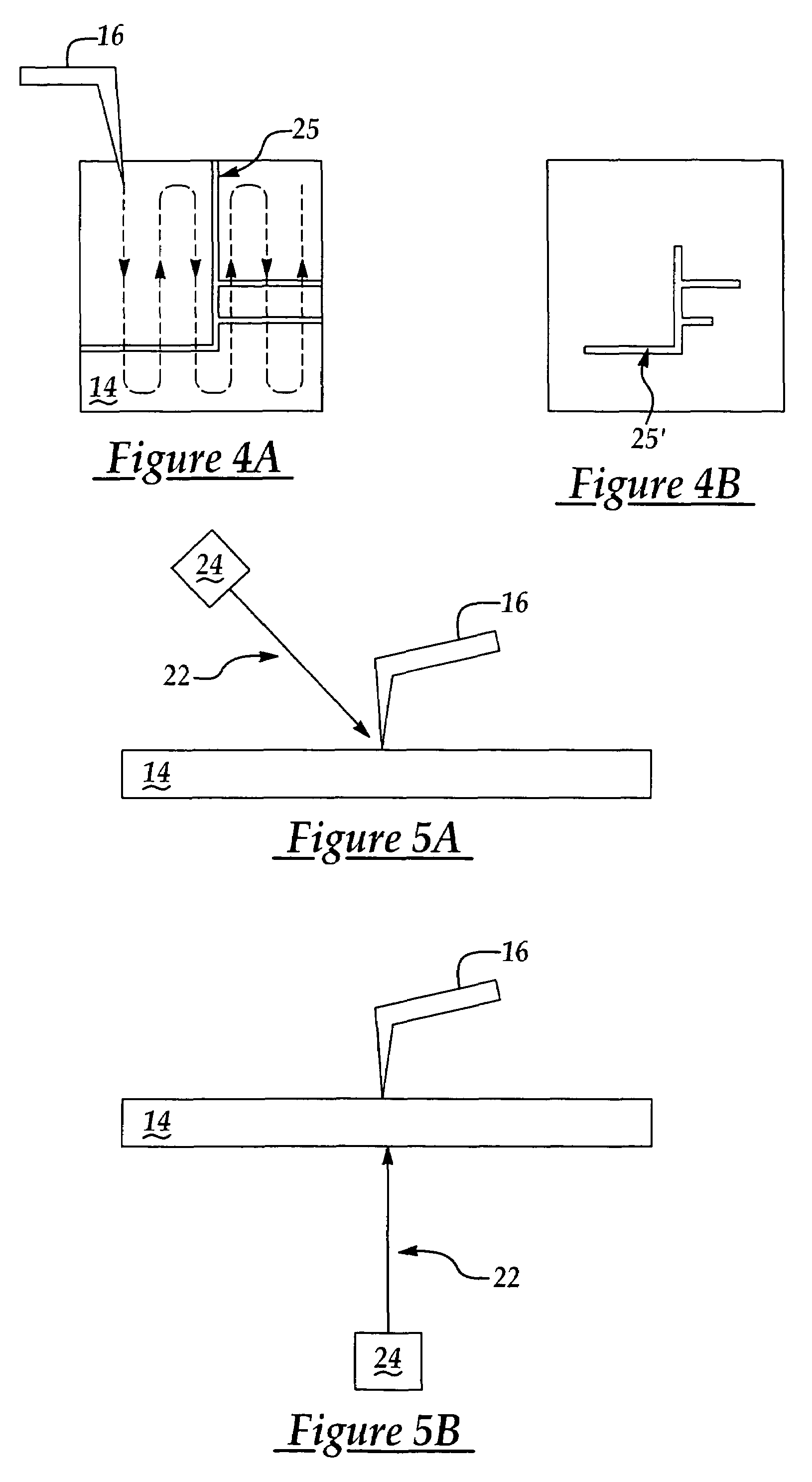
[0021]The invention provides an apparatus and a method for accurately and efficiently electrically testing a microelectronic product. The invention realizes the foregoing object within the context of a apparatus comprising: (1) an electrical test head to which is mated a microelectronic product for electrically testing the microelectronic product; and (2) a movable electrical probe tip positioned with respect to the electrical test head such as to movably electrically stress a portion of the microelectronic product other than an electrical contact portion of the microelectronic product. By employing within the invention the additional electrical probe tip bias stressing when electrically testing the microelectronic product, the microelectronic product may be more accurately and efficiently tested.

[0022]FIG. 1 shows a schematic diagram of an apparatus 10 in accord with the preferred embodiment of the invention.

[0023]The apparatus 10 comprises an electrical test head 12 which will gen...


PUM


Abstract

An apparatus and a method for electrically testing a microelectronic product employ an electrical probe tip for electrically stressing a portion of the microelectronic product other than an electrical contact portion of the microelectronic product when electrically testing the microelectronic product. The apparatus and the method provide for more accurate and efficient electrical testing of the microelectronic product.

Description

BACKGROUND OF THE INVENTION[0001]1. Field of the Invention[0002]The invention relates generally to methods for testing microelectronic products. More particularly, the invention relates to methods for efficiently testing microelectronic products.[0003]2. Description of the Related Art[0004]Integral to the fabrication of microelectronic products is the electrical testing of microelectronic products. The electrical testing of microelectronic products is undertaken for purposes of assuring the reliability and functionality of microelectronic products.[0005]While the electrical testing of microelectronic products is essential for their fabrication, such electrical testing is nonetheless not entirely without problems. In that regard, it is often difficult to accurately and efficiently electrically test microelectronic products. It is towards the foregoing object that the invention is directed.[0006]Various electrical test apparatus and methods have been disclosed in microelectronic produ...

Claims


Application Information

Patent Timeline
29 May 2007
Publication
US7224173B2
IPC
G01R31/305; G01R31/02; G01R31/26; G01R31/28
CPC
G01R31/2886
Inventors
HUNG, HUI-CHUAN