Column analog-to-digital conversion apparatus and method supporting a high frame rate in a sub-sampling mode

a conversion apparatus and sub-sampling technology, applied in the field of complementary metaloxide semiconductor (cmos) image sensor collumn analog-to-digital conversion apparatus and a conversion method capable of supporting a high frame rate in a sub-sampling mode, can solve the problems of high power consumption, inability to reduce the time needed to perform the analog-to-digital conversion of one horizontal line, and inability to reduce the structur

Inactive Publication Date: 2007-06-12
SAMSUNG ELECTRONICS CO LTD
View PDF11 Cites 29 Cited by
  • Summary
  • Abstract
  • Description
  • Claims
  • Application Information

AI Technical Summary

Problems solved by technology

Although the single ADC scheme can reduce chip area, it has high power consumption as compared to the column ADC scheme because it operates at high speed.
However, in the sub-sampling mode, the column ADC structure cannot reduce time in the X-direction (refer to FIG. 3) because of its structural characteristics.
The time needed to perform the analog-to-digital conversion of one horizontal line cannot be reduced.
The CMOS image sensor with the column ADC structure cannot reduce a horizontal line time because it uses independent ADC circuits in each of the columns.

Method used


Image

  • Column analog-to-digital conversion apparatus and method supporting a high frame rate in a sub-sampling mode
  • Column analog-to-digital conversion apparatus and method supporting a high frame rate in a sub-sampling mode
  • Column analog-to-digital conversion apparatus and method supporting a high frame rate in a sub-sampling mode

Examples


Embodiment Construction

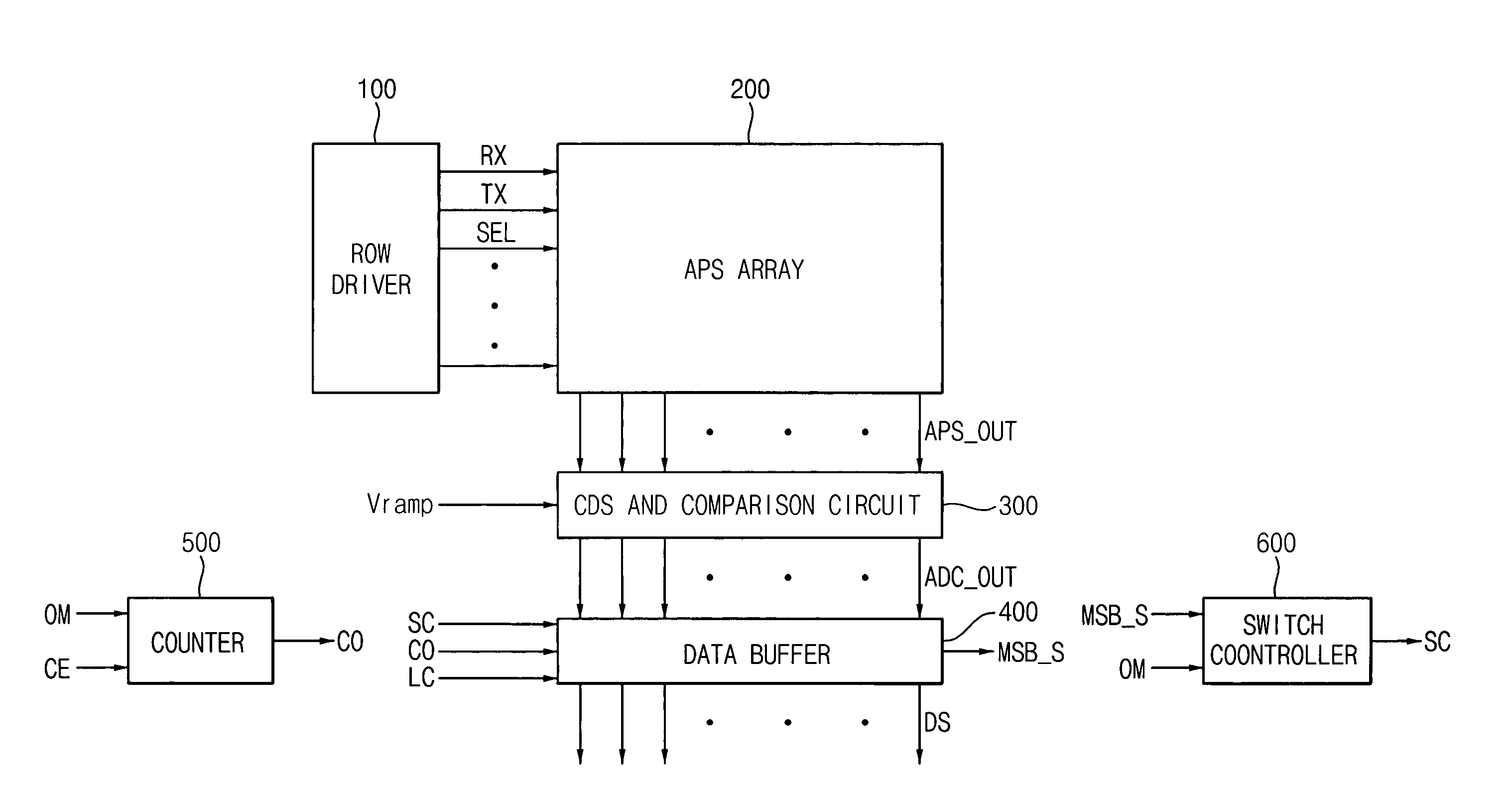
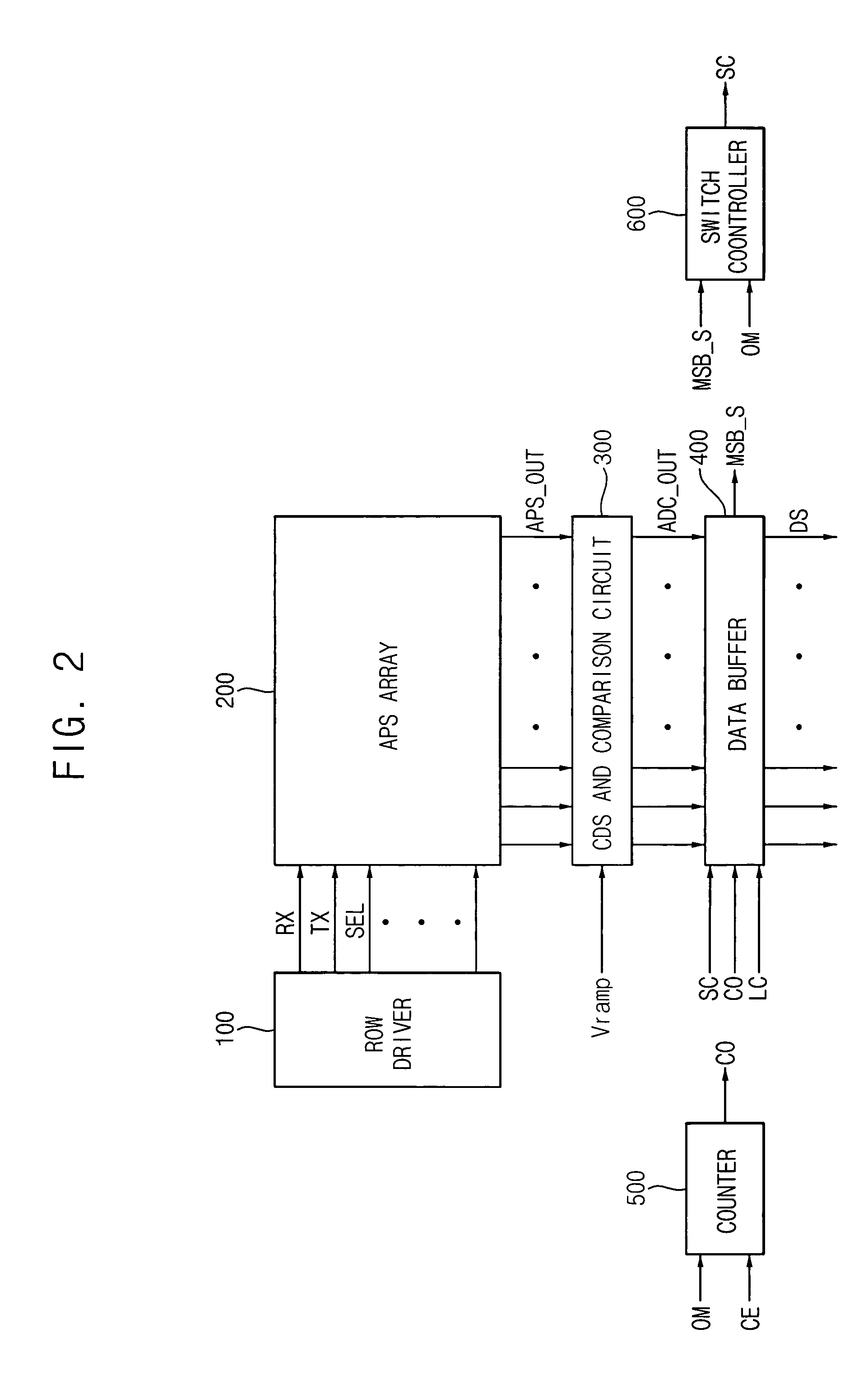
[0029]FIG. 2 is a block diagram illustrating a column-parallel type complementary metal-oxide semiconductor (CMOS) image sensor including an analog-to-digital conversion apparatus according to an exemplary embodiment of the present invention.

[0030]Referring to FIG. 2, the CMOS image sensor according to an exemplary embodiment of the present invention includes a row driver 100, an APS array 200, a correlated double sampling (CDS) and comparison circuit 300, a data buffer 400, a counter 500, and a switch controller 600.

[0031]The row driver 100 generates control signals RX, TX and SEL for controlling pixels of the APS array 200. The APS array 200 outputs corresponding pixel output signals APS_OUT via columns.

[0032]The CDS and comparison circuit 300 performs a CDS operation on the pixel output signals APS_OUT outputted by the APS array 200, performs a comparing operation on results of the CDS operation by using a ramp voltage Vramp, and outputs comparison result signals ADC_OUT via the ...


PUM


Abstract

A column analog-to-digital conversion apparatus includes a first correlated double sampling (CDS) and comparison unit of a CDS and comparison circuit for generating a first comparison result signal in response to a first pixel output signal and a ramp signal, a second CDS and comparison unit of the CDS and comparison circuit for generating a second comparison result signal in response to the first pixel output signal and the ramp signal in a sub-sampling mode, and a data buffer for determining a code value of a most significant bit (MSB) based on the second comparison result signal, determining code values of remaining lower bits based on a counting value outputted from a counter, and generating a digital code including the MSB and the remaining lower bits.

Description

CROSS-REFERENCE TO RELATED APPLICATIONS[0001]This application claims the benefit of Korean Patent Application No. 2005-41605 filed on May 18, 2005 in the Korean Intellectual Property Office (KIPO), the contents of which are herein incorporated by reference in its entirety.BACKGROUND OF THE INVENTION[0002]1. Field of the Invention[0003]The present invention relates to a column analog-to-digital conversion apparatus of a complementary metal-oxide semiconductor (CMOS) image sensor (CIS), and more particularly to a column analog-to-digital conversion apparatus and a method capable of supporting a high frame rate in a sub-sampling mode.[0004]2. Description of Related Art[0005]Compared with charge-coupled devices (CCDs), complementary metal-oxide semiconductor (CMOS) image sensors (CISs) operate at low voltages and have low power consumption. Also, the CMOS image sensors may be implemented in applications needing high-density integration using standard CMOS processes. For these reasons, t...

Claims


Application Information

Patent Timeline
Patent Type & Authority Patents(United States)
IPC IPC(8): H03M1/12
CPCH04N5/3456H04N5/3458H04N5/3575H04N5/3745H04N25/445H04N25/616H04N25/447H04N25/77H03M1/12
Inventor LIM, SU-HUN
Owner SAMSUNG ELECTRONICS CO LTD
Why Eureka
Try Eureka