Methods for using a silylation technique to reduce cell pitch in semiconductor devices

a technology of cell pitch and semiconductor devices, applied in semiconductor devices, photomechanical treatment, instruments, etc., can solve the problems of limiting the size and density with which semiconductor devices may be fabricated, the photolithography process limits the minimum achievable widths which can be obtained for the features of such conventional semiconductor devices, and the photolithography process limits the minimum achievable widths. , to achieve the effect of reducing the cell pitch of the formed device, reducing the cell pitch of the semiconductor device, and simple and feasibl

Inactive Publication Date: 2007-08-07
MACRONIX INT CO LTD
View PDF10 Cites 23 Cited by
  • Summary
  • Abstract
  • Description
  • Claims
  • Application Information

AI Technical Summary

Benefits of technology

[0008]The present invention addresses these needs by providing simple and feasible methods for using photoresist silylation techniques to reduce cell pitch in semiconductor devices. The cell pitch of the formed devices can be reduced using current lithography processes to, for example, half that of conventional devices. Since the cell pitch of the semiconductor devices can be reduced, device densities can be increased, resulting in smaller and faster integrated circuits.

Problems solved by technology

Typical photolithography processes, however, limit the size and density with which semiconductor devices may be fabricated.
Consequently, the photolithography process limits the minimum achievable widths which can be obtained for those features of such conventional semiconductor devices.
It therefore can be difficult to reduce the widths of and distances between, for example, transistor gate conductors that are defined by the photolithography process.
Because of limitations of the photolithography process, the pitch of semiconductor devices, such as for example transistor devices, cannot be easily reduced.
Since the pitch of semiconductor devices cannot be easily reduced, the device density cannot easily be increased to meet the high demand for smaller and faster semiconductor devices.

Method used


Image

  • Methods for using a silylation technique to reduce cell pitch in semiconductor devices
  • Methods for using a silylation technique to reduce cell pitch in semiconductor devices
  • Methods for using a silylation technique to reduce cell pitch in semiconductor devices

Examples


Embodiment Construction

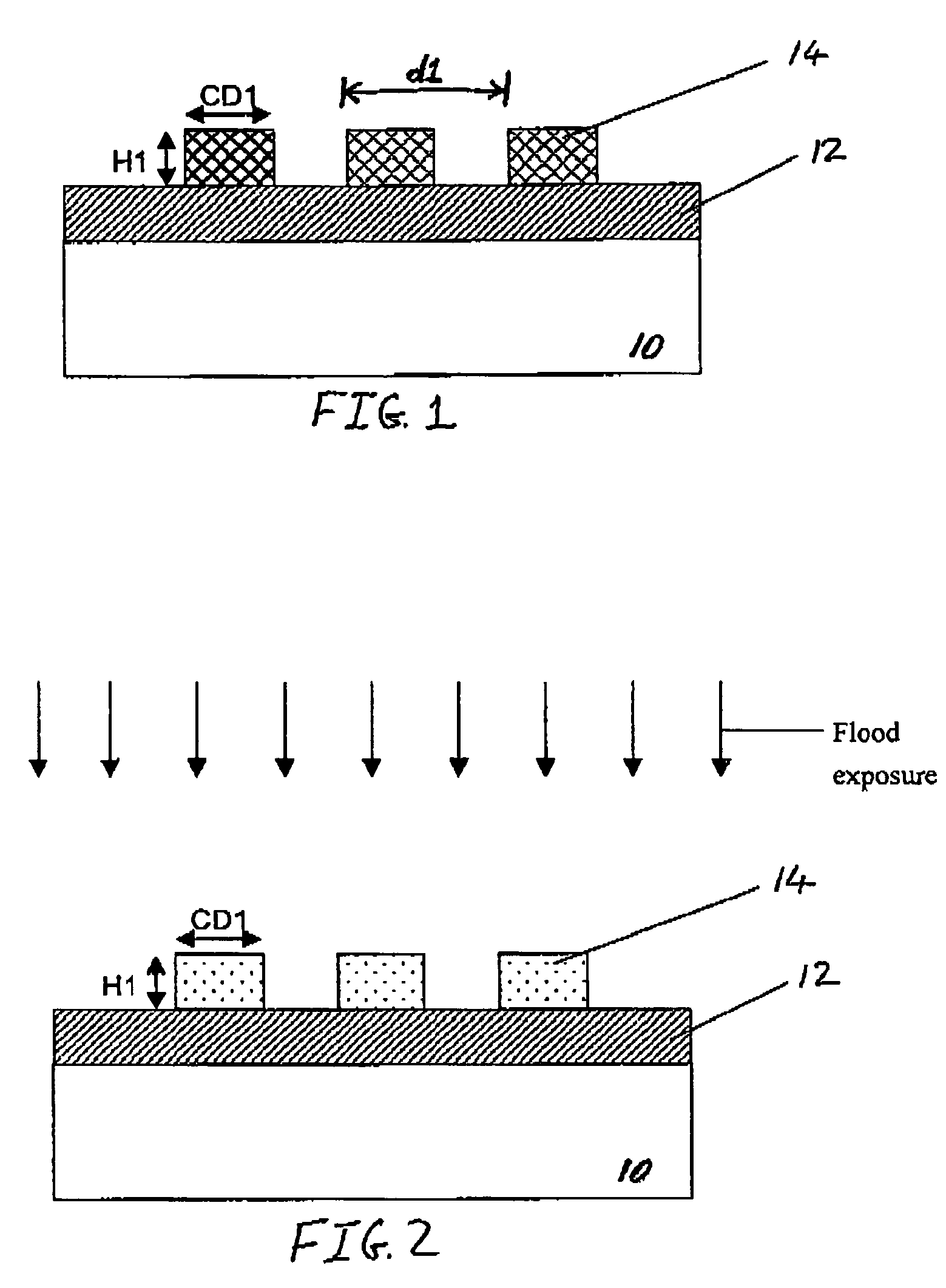
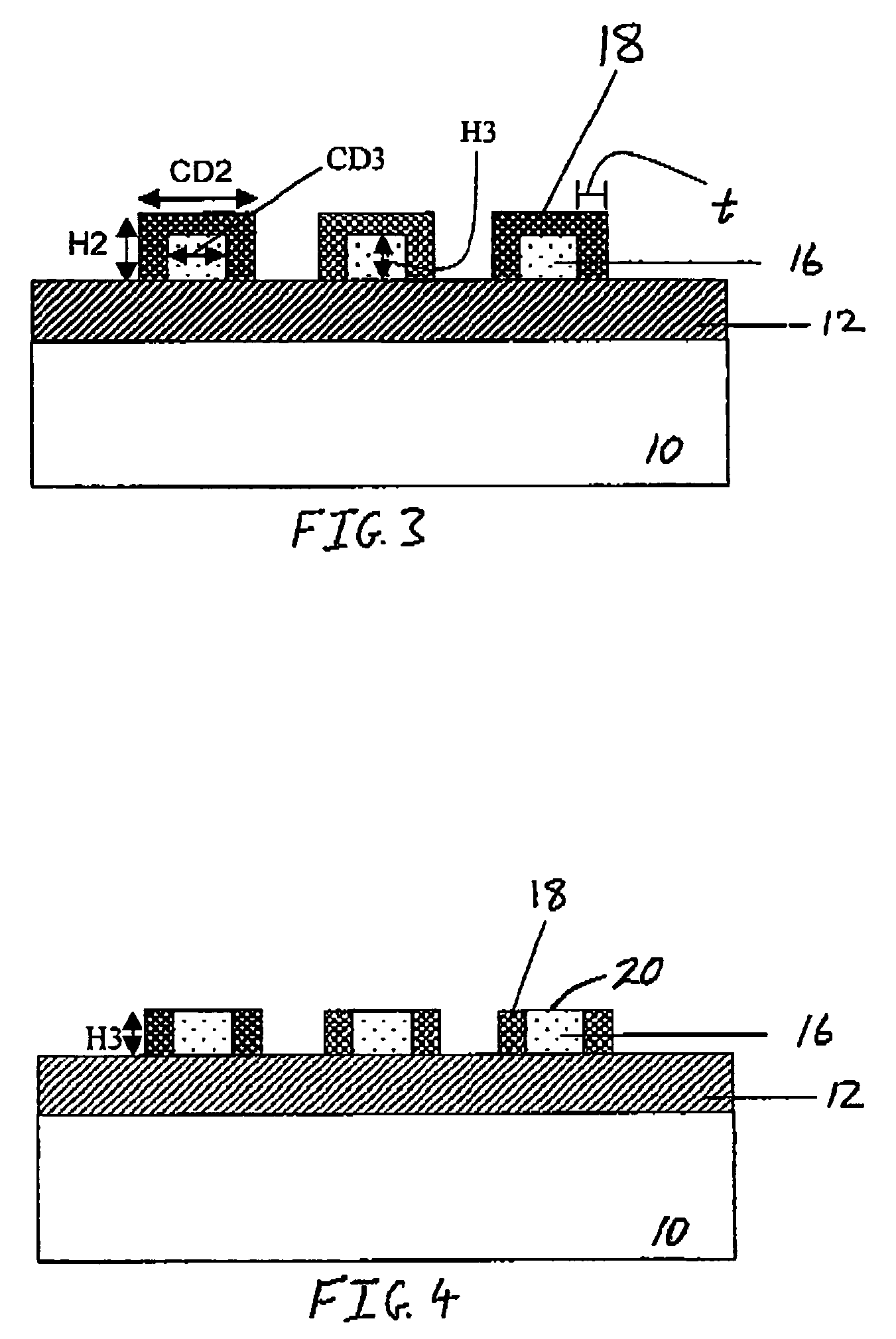
[0020]Reference will now be made in detail to the presently preferred embodiments of the invention, examples of which are illustrated in the accompanying drawings. Wherever possible, the same or similar reference numbers are used in the drawings and the description to refer to the same or like parts. It should be noted that the drawings are in simplified form and are not to precise scale. In reference to the disclosure herein, for purposes of convenience and clarity only, directional terms, such as, top, bottom, left, right, up, down, over, above, below, beneath, rear, and front, are used with respect to the accompanying drawings. Such directional terms should not be construed to limit the scope of the invention in any manner.

[0021]Although the disclosure herein refers to certain illustrated embodiments, it is to be understood that these embodiments are presented by way of example and not by way of limitation. The intent of the following detailed description, although discussing exe...


PUM

PropertyMeasurementUnit
thicknessaaaaaaaaaa
distancesaaaaaaaaaa
sizeaaaaaaaaaa

Abstract

A method for forming a semiconductor device having a reduced pitch is provided. The method includes providing a substrate, forming a material layer over the substrate, forming a photoresist layer over the material layer, exposing a top surface of the photoresist layer to radiation, and forming a silylated layer over the photoresist layer. The method further includes removing a portion of the silylated layer to expose the photoresist layer, removing the photoresist layer, removing portions of the material layer using the silylated layer as a mask, and removing another portion of the silylated layer.

Description

BACKGROUND OF THE INVENTION[0001]1. Field of the Invention[0002]The present invention relates generally to methods for fabricating semiconductor devices and, more particularly, to methods for reducing cell pitch in semiconductor devices.[0003]2. Description of Related Art[0004]The fabrication of semiconductor devices is a complex process, which typically includes a number of photolithography processes. In a typical photolithography process, a photoresist material is deposited over a layer to be patterned and is exposed to a radiation source, such as, for example, ultraviolet radiation, which is projected through a mask that defines the pattern to be formed in the photoresist. The mask only passes radiation to selected regions of the layer to be patterned, resulting in the exposure of the photoresist only at those selected regions. The photoresist is then developed to form a patterned photoresist layer over the underlying layer to be patterned. The portions of the underlying layer le...

Claims


Application Information

Patent Timeline
Patent Type & Authority Patents(United States)
IPC IPC(8): H01L21/311G03F7/40H01L21/027H01L21/033H01L21/28H01L21/302H01L21/461
CPCG03F7/405H01L21/0273H01L21/0332H01L21/0337H01L21/0338H01L21/28123
Inventor CHENG, YANG CHIN
Owner MACRONIX INT CO LTD
Why Eureka
Try Eureka