Trench VDMOS device with integrated ESD protection and manufacturing method

A technology for ESD protection and devices, applied in semiconductor/solid-state device manufacturing, semiconductor devices, electric solid-state devices, etc., can solve problems such as large substrate coupling noise, obvious parasitic effects, and large drain-source current

Active Publication Date: 2020-11-06
ZHUHAI MAIJU MICROELECTRONICS CO LTD
View PDF5 Cites 0 Cited by
  • Summary
  • Abstract
  • Description
  • Claims
  • Application Information

AI Technical Summary

Problems solved by technology

ESD protection structures such as diodes formed of polysilicon / bulk silicon and bulk silicon diodes are relatively simple to implement, but they have disadvantages such as large drain-source current, obvious parasitic effects, and large substrate coupling noise, which will cause damage to the device and is not conducive to the protection of the device. normal work

Method used


Image

  • Trench VDMOS device with integrated ESD protection and manufacturing method
  • Trench VDMOS device with integrated ESD protection and manufacturing method
  • Trench VDMOS device with integrated ESD protection and manufacturing method

Examples


Embodiment 1

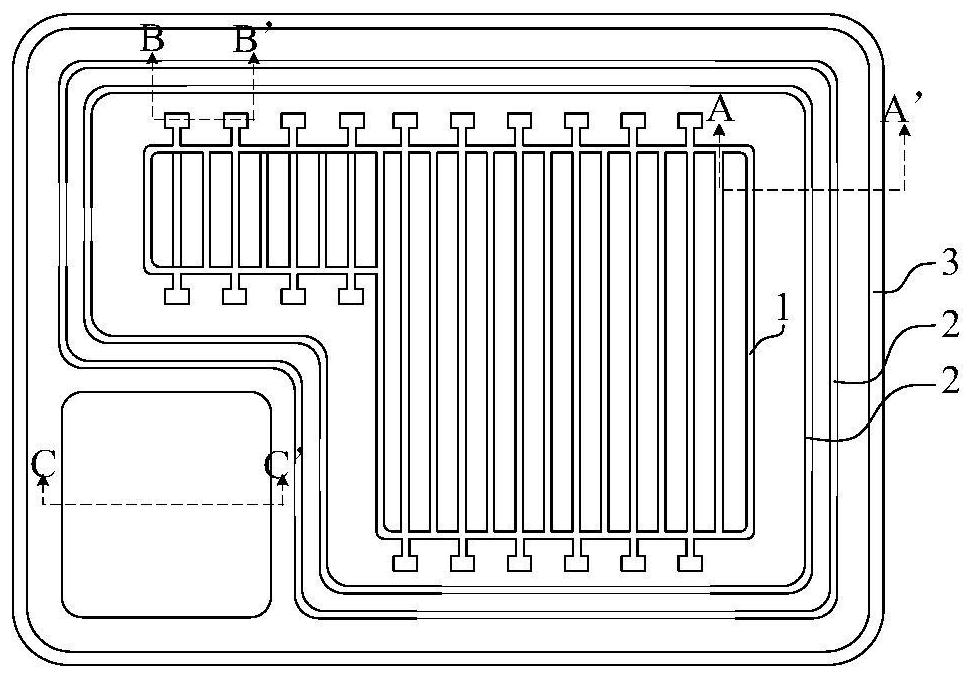
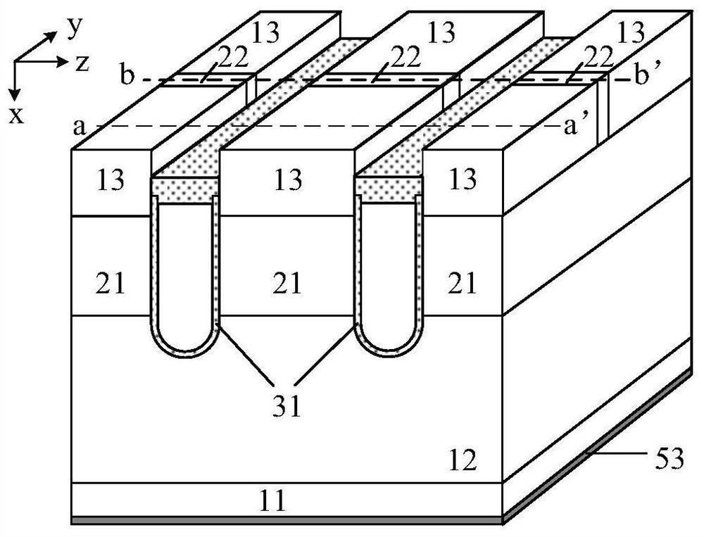
[0062] A Trench VDMOS device with integrated ESD protection, including a Trench VDMOS structure and an ESD protection structure;

[0063] The Trench VDMOS structure includes a cell area and a terminal protection area, the cell area includes a plurality of cells with the same structure and sequentially connected, the cell area includes a first conductivity type substrate 11, and is located between the first conductivity type substrate 11 The drift region 12 of the first conductivity type on the top, the well region 21 of the second conductivity type located above the drift region 12 of the first conductivity type, the source contact region 13 of the first conductivity type located above the well region 21 of the second conductivity type and the second conductivity type The source contact region 22 of the second conductivity type, the source metal 51 is located above the pre-metal dielectric 32 and is in contact with the source contact region 22 of the second conductivity type an...

Embodiment 2

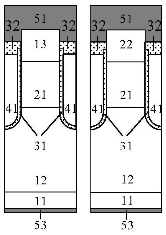
[0090] Figure 7 The Trench VDMOS sectional view provided in Embodiment 2 is different from Embodiment 1 in that the source contact region 13 of the first conductivity type is arranged above the source contact region 13 of the second conductivity type and the source contact region 22 of the second conductivity type. .

Embodiment 3

[0092] Figure 8 The difference between the Trench VDMOS sectional view provided in Embodiment 3 and Embodiment 2 is that a metal silicide 00 is disposed above the source contact region 13 of the first conductivity type.


PUM


Abstract

The invention provides a Trench VDMOS device with integrated ESD protection and a manufacturing method thereof. The Trench VDMOS device comprises a Trench VDMOS structure and an ESD protection structure. The Trench VDMOS structure comprises a cellular region and a terminal protection region. The terminal protection region adopts a trench structure and comprises a cutoff ring and at least one pressure dividing ring. The ESD protection structure comprises multiple Zener diode cells. The ESD protection structure is connected on the two ends of the gate metal and the source metal. The Trench VDMOSreduces the Trench VDMOS specific on resistance by reducing the cell pitch and increasing the contact area of the source metal and the first conductivity type source. In addition, the ESD protectionstructure is located on the hard mask SiO2 and isolated from the Trench VDMOS unit and is compatible with the Trench VDMOS manufacturing process so that the active region photolithography plate is reduced and the manufacturing cost is reduced without affecting the device performance.

Description

technical field [0001] The invention belongs to the technical field of semiconductor power devices, and relates to an integrated ESD protection Trench VDMOS device and a manufacturing method thereof. Background technique [0002] Trench power MOS devices have the characteristics of high integration, low on-resistance, fast switching speed, and low switching loss. They are widely used in various power management and switching conversions, and have broad development and application prospects. For trench power MOS, reducing the cell pitch can significantly reduce the specific on-resistance, but due to the limited contact hole size and overlay deviation, the size of the trench power MOS cannot be further reduced. At the same time, with the increase of the cell pitch Shrinking, the source contact resistance of the device increases, affecting the total on-resistance of the power MOS. [0003] The thickness of the gate oxide layer of the trench power MOS is relatively thin. This s...

Claims


Application Information

Patent Timeline
Patent Type & Authority Patents(China)
IPC IPC(8): H01L27/02H01L29/78H01L29/06H01L21/336
CPCH01L27/0203H01L29/0603H01L29/0684H01L29/66712H01L29/7803
Inventor 乔明何林蓉周号
Owner ZHUHAI MAIJU MICROELECTRONICS CO LTD
Why Eureka
Try Eureka