Longitudinal floating field plate device with charge balance voltage withstanding layer and manufacturing method thereof

A technology of charge balance and withstand voltage layer, applied in semiconductor/solid-state device manufacturing, electrical components, semiconductor devices, etc., can solve the problem that the device performance needs to be further improved

Inactive Publication Date: 2019-11-29
UNIV OF ELECTRONICS SCI & TECH OF CHINA
View PDF4 Cites 6 Cited by
  • Summary
  • Abstract
  • Description
  • Claims
  • Application Information

AI Technical Summary

Problems solved by technology

However, the existing vertical floating field plate structure has not introduced other technical means to optimize the trade-off relationship between withstand voltage and specific conductance, and the device performance needs to be further improved.

Method used


Image

  • Longitudinal floating field plate device with charge balance voltage withstanding layer and manufacturing method thereof
  • Longitudinal floating field plate device with charge balance voltage withstanding layer and manufacturing method thereof
  • Longitudinal floating field plate device with charge balance voltage withstanding layer and manufacturing method thereof

Examples


Embodiment 1

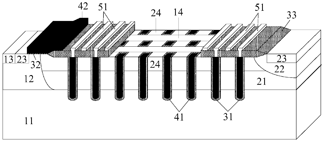
[0043] A vertical floating field plate device with a charge balance withstand voltage layer, comprising:

[0044] First conductivity type semiconductor substrate 11, first conductivity type well region 12, first conductivity type semiconductor contact region 13, first conductivity type charge balance withstand voltage layer 14, second conductivity type drift region 21, second conductivity type well Region 22, second conductivity type semiconductor contact region 23, second conductivity type charge balance withstand voltage layer 24, first dielectric oxide layer 31, second dielectric oxide layer 32, third dielectric oxide layer 33, floating field plate polysilicon electrode 41. Control gate polysilicon electrode 42, metal strip 51;

[0045] Wherein, the drift region 21 of the second conductivity type is located above the semiconductor substrate 11 of the first conductivity type, the well region 12 of the first conductivity type is located on the left side of the drift region 21...

Embodiment 2

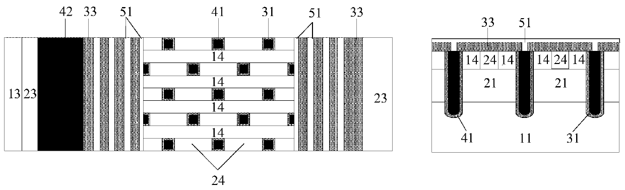
[0069] Such as image 3 As shown, it is a schematic structural diagram of the vertical floating field plate device with a charge balance withstand voltage layer in Embodiment 2. The difference between this example and the structure of Embodiment 1 is that the first conductivity type charge balance withstand voltage layer 14 The super junction structure formed with the charge balance withstand voltage layer 24 of the second conductivity type is located in the body instead of on the surface, and can further modulate the electric field in the drift region to improve the withstand voltage of the device, and its working principle is basically the same as that of Embodiment 1.

Embodiment 3

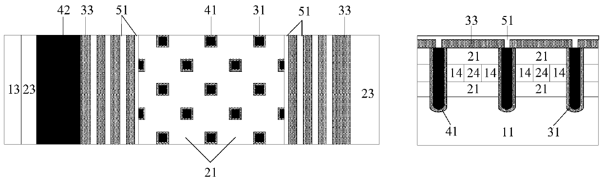
[0071] Such as Figure 4 As shown, it is a schematic structural diagram of the vertical floating field plate device with a charge balance withstand voltage layer of embodiment 3. The difference between this example and the structure of embodiment 1 is that the first conductivity type charge balance withstand voltage layer 14 The super junction structure formed with the second conductivity type charge balance withstand voltage layer 24 is arranged alternately left and right in the horizontal direction, and its working principle is basically the same as that of the first embodiment.


PUM


Abstract

The invention provides a longitudinal floating field plate device with a charge balance voltage withstanding layer and a manufacturing method. The device comprises a first conductive-type semiconductor substrate, a first conductive-type well region, a first conductive-type semiconductor contact region, a first conductive-type charge balance voltage withstanding layer, a second conductive-type drift region, a second conductive-type well region, a second conductive-type semiconductor contact region, a second conductive-type charge balance voltage withstanding layer, a first dielectric oxide layer, a second dielectric oxide layer, a third dielectric oxide layer, a floating field plate polycrystalline silicon electrode, a control gate polycrystalline silicon electrode and a metal strip, wherein the first dielectric oxide layer and the floating field plate polycrystalline silicon electrode form a longitudinal floating field plate. A super-junction structure composed of the first conductive-type charge balance voltage withstanding layer and the second conductive-type charge balance voltage withstanding layer is introduced to the second conductive-type drift region of the device, the electric field of the drift region is modulated, a low-resistance current path is provided, so that the voltage withstanding performance of the device is improved, and the specific on-resistance of the device is reduced.

Description

technical field [0001] The invention belongs to the field of power semiconductors, and mainly provides a vertical floating field plate device with a charge balance withstand voltage layer and a manufacturing method thereof. Background technique [0002] Power semiconductor devices have been widely used in consumer electronics, computers and peripherals, network communications, electronic special equipment and instruments, automotive electronics, LED Display and electronic lighting and many other aspects. Because the source, gate, and drain of the device are all on the chip surface, it is easy to integrate with other devices and circuits through internal connections, and is widely used in power integrated circuits. The vertical floating field plate device introduces a vertical floating field plate in the drift region, which reduces the specific on-resistance while increasing the withstand voltage of the device. However, the existing vertical floating field plate structure h...

Claims


Application Information

Patent Timeline
Patent Type & Authority Applications(China)
IPC IPC(8): H01L29/06H01L29/40H01L29/739H01L21/331
CPCH01L29/0634H01L29/404H01L29/407H01L29/66325H01L29/7393
Inventor 章文通何俊卿杨昆王睿张森乔明张波李肇基
Owner UNIV OF ELECTRONICS SCI & TECH OF CHINA
Why Eureka
Try Eureka