4H-SiC MOSFET power device and manufacturing method thereof

A technology of power devices and epitaxial layers, applied in semiconductor/solid-state device manufacturing, semiconductor devices, electrical components, etc., can solve problems such as device failure, gate oxide breakdown, etc., to improve current capability, reduce electric field strength, and improve reliability. sexual effect

Active Publication Date: 2019-04-12
INST OF MICROELECTRONICS CHINESE ACAD OF SCI
View PDF4 Cites 6 Cited by
  • Summary
  • Abstract
  • Description
  • Claims
  • Application Information

AI Technical Summary

Problems solved by technology

However, there are still many problems in the power devices of SiC materials.
Taking SiC MOSFET as an example, the dielectric constant of SiC is about 10, the critical breakdown electric field is about 3MV / cm, and SiO 2 The dielectric constant is about 3.9, by Gauss's theorem k SiC E. SiC =k SiO2 E. SiO2 know SiO 2 The electric field strength that the layer needs to withstand is about 7.7MV / cm. Such a high electric field strength will easily cause the gate oxide layer to break down in advance, resulting in device failure.

Method used


Image

  • 4H-SiC MOSFET power device and manufacturing method thereof

Examples


Embodiment Construction

[0039] In order to make the object, technical solution and advantages of the present invention clearer, the present invention will be further described in detail below in conjunction with specific embodiments and with reference to the accompanying drawings.

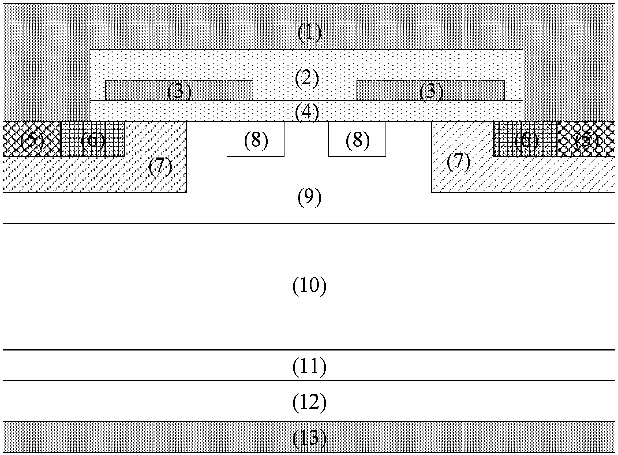
[0040] Such as figure 1 Shown is a schematic structural diagram of a 1200V 4H-SiC MOSFET power device proposed by an embodiment of the present invention, which has a vertical conductive structure. The power device includes a source 1, SiO 2 Interlayer dielectric 2, gate 3, gate oxide layer 4, P+ contact region 5, N+ source region 6, P well 7, additional implanted P-type region 8, N-type epitaxial layer 9, N- epitaxial layer 10, buffer layer 11. N+ substrate 12 and drain 13. in:

[0041] The drain 13 is formed on the back of the substrate 12 by sputtering metal Ni, and annealed at 900° C.-1000° C. for 4-6 minutes to form an ohmic contact. In this embodiment, the annealing temperature is 900° C., and the annealing time i...


PUM


Abstract

The invention discloses a 4H-SiC MOSFET power device and a manufacturing method thereof. The power device comprises a source electrode (1), an SiO2 interlayer dielectric (2), a grid electrode (3), a gate oxide layer (4), a P + contact region (5), an N+ source region (6), a P well (7), an additionally injected P-type region (8), an N type epitaxial layer (9), an N-epitaxial layer (10), a buffer layer (11), an N+ substrate (12) and a drain electrode (13). The 4H-SiC MOSFET power device disclosed in the invention adopts a separation grid structure, and by virtue of the structure the input capacitance and the grid leakage capacitance can be effectively lowered, and the switching performance of the device is improved; by introducing P type doping in a JFET region, the electric field intensity of a gate oxide layer can be effectively reduced, and the reliability of the device is improved; and in addition, a current expanding layer structure is adopted, so that the current capability of the device can be considered.

Description

technical field [0001] The invention relates to the technical field of power semiconductors, in particular to a 4H-SiC MOSFET power device and a manufacturing method thereof. Background technique [0002] SiC material is a typical representative of the third-generation wide-bandgap semiconductor material. Due to its advantages such as high critical breakdown electric field strength, high carrier saturation drift velocity, and high thermal conductivity, it has become a high-power , high temperature, high frequency, ideal material for radiation resistant devices. [0003] After more than 20 years of rapid development, SiC power devices have achieved impressive results. For example, 600V, 1200V, 1700V, 3300V, and 10kV SiC MOSFET devices have been successfully developed, and 600V, 1200V, and 1700V SiC MOSFET devices have been commercialized. However, power devices of SiC materials still have many problems. Taking SiC MOSFET as an example, the dielectric constant of SiC is abou...

Claims


Application Information

Patent Timeline
Patent Type & Authority Applications(China)
IPC IPC(8): H01L29/78H01L21/336H01L29/423H01L29/06H01L29/16
CPCH01L29/0603H01L29/0684H01L29/1608H01L29/42356H01L29/66477H01L29/78
Inventor 宋瓘白云陈宏汤益丹杨成樾田晓丽陆江刘新宇
Owner INST OF MICROELECTRONICS CHINESE ACAD OF SCI
Why Eureka
Try Eureka