Low-resistance device with equipotential floating grooves and manufacturing method of low-resistance device

A floating and equipotential technology, used in semiconductor/solid-state device manufacturing, semiconductor devices, electrical components, etc., can solve problems such as larger than on-resistance, and achieve the effects of high withstand voltage, increased withstand voltage, and large average electric field

Active Publication Date: 2021-01-01
UNIV OF ELECTRONICS SCI & TECH OF CHINA +1
View PDF5 Cites 6 Cited by
  • Summary
  • Abstract
  • Description
  • Claims
  • Application Information

AI Technical Summary

Problems solved by technology

However, the specific on-resistance of traditional dielectric trench LDMOS is still relatively large, which fails to further alleviate the contradiction between withstand voltage and specific on-resistance

Method used


Image

  • Low-resistance device with equipotential floating grooves and manufacturing method of low-resistance device
  • Low-resistance device with equipotential floating grooves and manufacturing method of low-resistance device
  • Low-resistance device with equipotential floating grooves and manufacturing method of low-resistance device

Examples


Embodiment 1

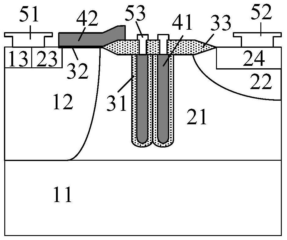
[0040] A kind of low-resistance device with equipotential floating slot described in embodiment 1, such as figure 1 shown, including:

[0041] First conductivity type semiconductor substrate 11, first conductivity type well region 12, first conductivity type source heavily doped region 13, second conductivity type drift region 21, second conductivity type well region 22, second conductivity type source Terminal heavily doped region 23, second conductivity type drain terminal heavily doped region 24, first dielectric oxide layer 31, second dielectric oxide layer 32, third dielectric oxide layer 33, floating field plate polysilicon electrode 41, control gate Polysilicon electrode 42, source metal 51, drain metal 52, metal strip 53;

[0042]Wherein, the drift region 21 of the second conductivity type is located above the semiconductor substrate 11 of the first conductivity type, the well region 12 of the first conductivity type is located on the left side of the drift region 21 ...

Embodiment 2

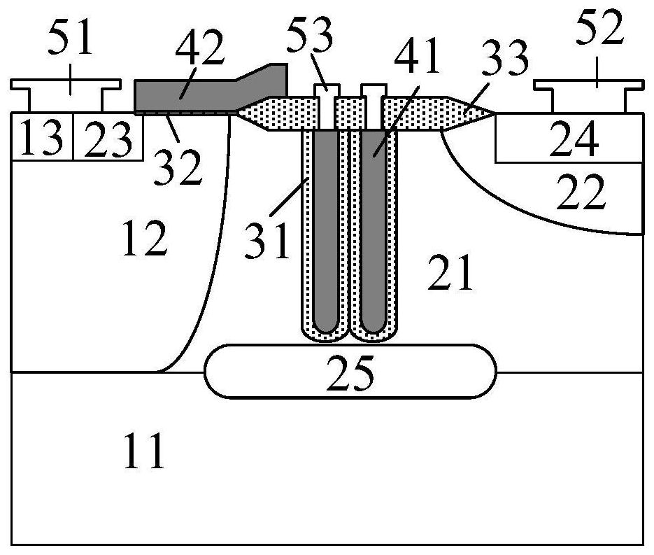
[0064] Such as figure 2 As shown, it is a schematic diagram of the structure of a low-resistance device with an equipotential floating slot in Example 2. The difference between this example and the structure of Example 1 is that the bottom of the vertical floating field plate is formed by ion implantation at the bottom of the slot The buried layer 25 of the second conductivity type. In this example, the buried layer 25 of the second conductivity type introduces a low-resistance conductive path at the bottom of the groove to further reduce the device resistance and increase the device current. Its working principle is basically the same as that of Embodiment 1.

Embodiment 3

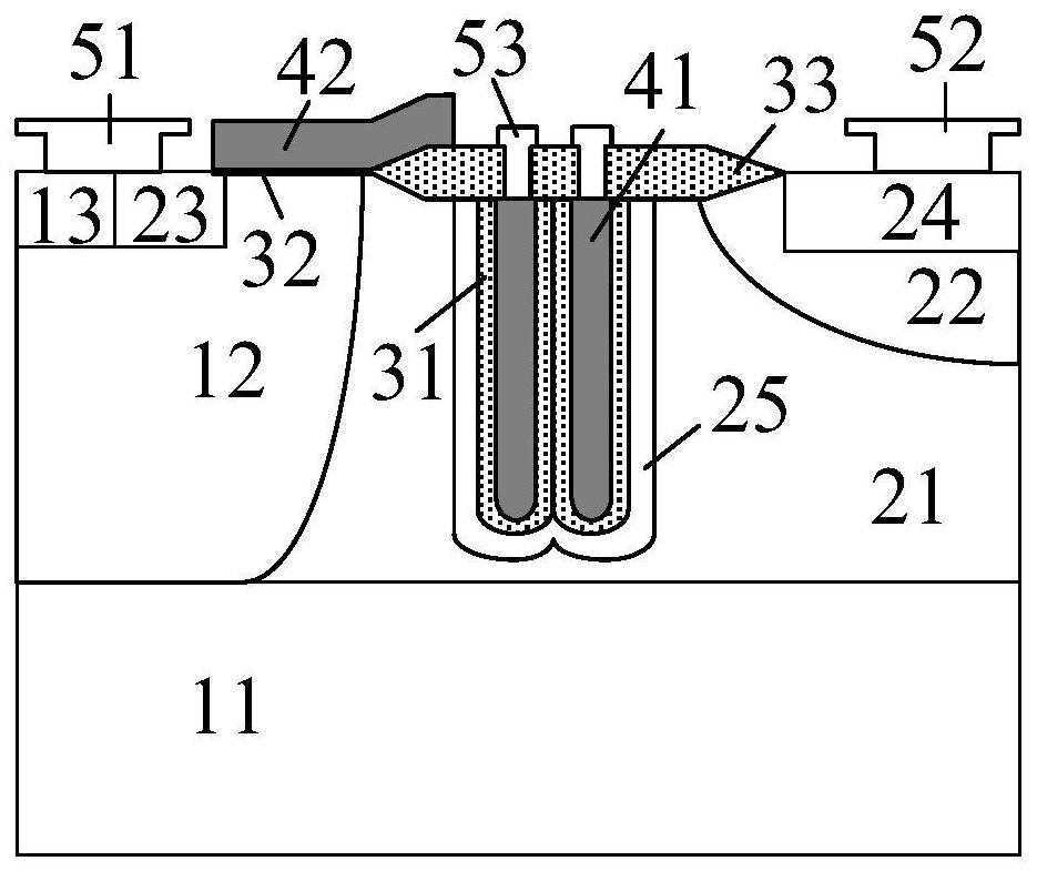
[0066] Such as image 3 As shown, it is a schematic diagram of the structure of a low-resistance device with an equipotential floating slot in Example 3. The difference between this example and the structure of Example 1 is that the periphery of the vertical floating field plate is formed by oblique implantation of the slot wall The second conductivity type doped strip 25 surrounding the vertical field plate structure, in this example, the second conductivity type doped strip 25 introduces a low-resistance conductive path around the vertical floating field plate, further reduces the device resistance, improves the device current, and its working The principle is basically the same as in Embodiment 1.


PUM


Abstract

The invention provides a low-resistance device with equipotential floating grooves, and the device comprises a first conductive type semiconductor substrate, a first conductive type well region, a first conductive type source end heavily doped region, a second conductive type drift region, a second conductive type well region, a second conductive type source end heavily doped region and a second conductive type drain end heavily doped region, a first dielectric oxide layer, a second dielectric oxide layer, a third dielectric oxide layer, a floating field plate polycrystalline silicon electrode, a control gate polycrystalline silicon electrode, source metal, drain metal and a metal strip; the first dielectric oxide layer and the floating field plate polycrystalline silicon electrode form alongitudinal floating field plate which is distributed in the whole second conductive type drift region; under the same length, the dielectric layer can bear higher breakdown voltage, the floating electrode can modulate the potential distribution of the drift region, so the potential distribution is uniform, the withstand voltage of the device is further improved, the floating field plate assistsin depletion, and the injection dose of the drift region can also be improved, so that the specific on-resistance is reduced.

Description

technical field [0001] The invention belongs to the field of power semiconductors, and mainly provides a low-resistance device with equipotential floating slots and a manufacturing method thereof. Background technique [0002] Power semiconductor devices have been widely used in consumer electronics, computers and peripherals, network communications, electronic special equipment and instruments, automotive electronics, LED Display and electronic lighting and many other aspects. Because the source, gate, and drain of lateral devices are all on the chip surface, they are easy to integrate with other devices and circuits through internal connections, and are widely used in power integrated circuits. In the design of lateral devices, the devices are required to have high breakdown voltage and low specific on-resistance. A higher breakdown voltage requires a device with a longer drift region length and a lower drift region doping concentration, but this also leads to an increas...

Claims


Application Information

Patent Timeline
Patent Type & Authority Applications(China)
IPC IPC(8): H01L29/78H01L29/40H01L21/336
CPCH01L29/7816H01L29/404H01L29/407H01L29/66681H01L29/7824H01L29/42368
Inventor 章文通祖健朱旭晗乔明李肇基张波
Owner UNIV OF ELECTRONICS SCI & TECH OF CHINA
Why Eureka
Try Eureka