Optical pulse demultiplexer and method thereof

a technology of optical pulse and multiplexer, which is applied in the field of optical pulse demultiplexer and method thereof, can solve the problems of difficult to adjust the polarization and phase into the optimum condition, and the inability to directly convert such an ultra high-speed optical pulse into an electric signal at the receiving terminal, so as to achieve improved pulse demultiplexing efficiency, and improved accuracy

Inactive Publication Date: 2007-08-21
NAT INST OF INFORMATION & COMM TECH
View PDF22 Cites 2 Cited by
  • Summary
  • Abstract
  • Description
  • Claims
  • Application Information

AI Technical Summary

Benefits of technology

[0010]With the above configurations of the invention, while an input pulse signal reciprocates in the saturable absorber, it receives pulse demultiplexing effects on both ways, and therefore a desired channel part can be accurately demultiplexed.
[0011]The pulse demultiplexing efficiency is even improved when an optical clock pulse and a pulse signal light transmit in the opposite directions in the saturable absorber compared to a case that they transmit in the same direction. Accordingly, the higher demultiplexing performance is realized when a pulse signal reciprocates in a saturable absorber compared to a case that pulse demultiplexing is merely performed twice in serial.
[0012]An optical pulse demultiplexer according to the invention, preferably, further comprises a first optical delay disposed between the optical band reflection mirror and the saturable absorber on the optical pass, and a second optical delay disposed between the optical clock generator and the optical band reflection mirror on the optical path. This configuration makes it easier to adjust the timing that each optical pulse of a pulse signal light of the signal wavelength λs enters the saturable absorber almost simultaneously with different optical pulses of the optical clock on the ways of going and returning.
[0016]As explained above, the pulse demultiplexing is performed twice in the saturable absorber since the input pulse signal light reciprocated in the saturable absorber and each optical pulse of the input pulse signal light enters the saturable absorber almost simultaneously with different optical pulses of the optical clock on the ways of going and retuning. With this operation, the pulse demultiplexing efficiency is improved and therefore a desired channel can be accurately demultiplexed.
[0017]The pulse demultiplexing efficiency is even improved when an optical clock pulse and a pulse signal light propagate in the opposite directions in the saturable absorber compared to a case that they propagate in the same direction. Accordingly, a higher demultiplexing efficiency can be realized when an optical pulse reciprocates in the saturable absorber compared to a case that the pulse demultiplexing is merely performed twice in serial.
[0018]According to the invention, a low-speed optical pulse signal is accurately demultiplexed from a high-speed optical pulse signal and in addition a higher demultiplexing performance is realized compared to a case that the pulse demultiplexing is performed twice in serial.

Problems solved by technology

It is impossible to directly convert such an ultra high-speed optical pulse into an electric signal at a receiving terminal.
Furthermore, since these conventional optically controlled optical switches use nonlinear interfering effects, the adjustment of polarization and the adjustment of phase are depending on each other and therefore there are a large number of pseudo optimum points.
Accordingly, it is very difficult to adjust the polarization and phase into the optimum condition.

Method used


Image

  • Optical pulse demultiplexer and method thereof
  • Optical pulse demultiplexer and method thereof
  • Optical pulse demultiplexer and method thereof

Examples


Embodiment Construction

[0024]Explanatory embodiments of the invention are explained below in detail with reference to the drawings.

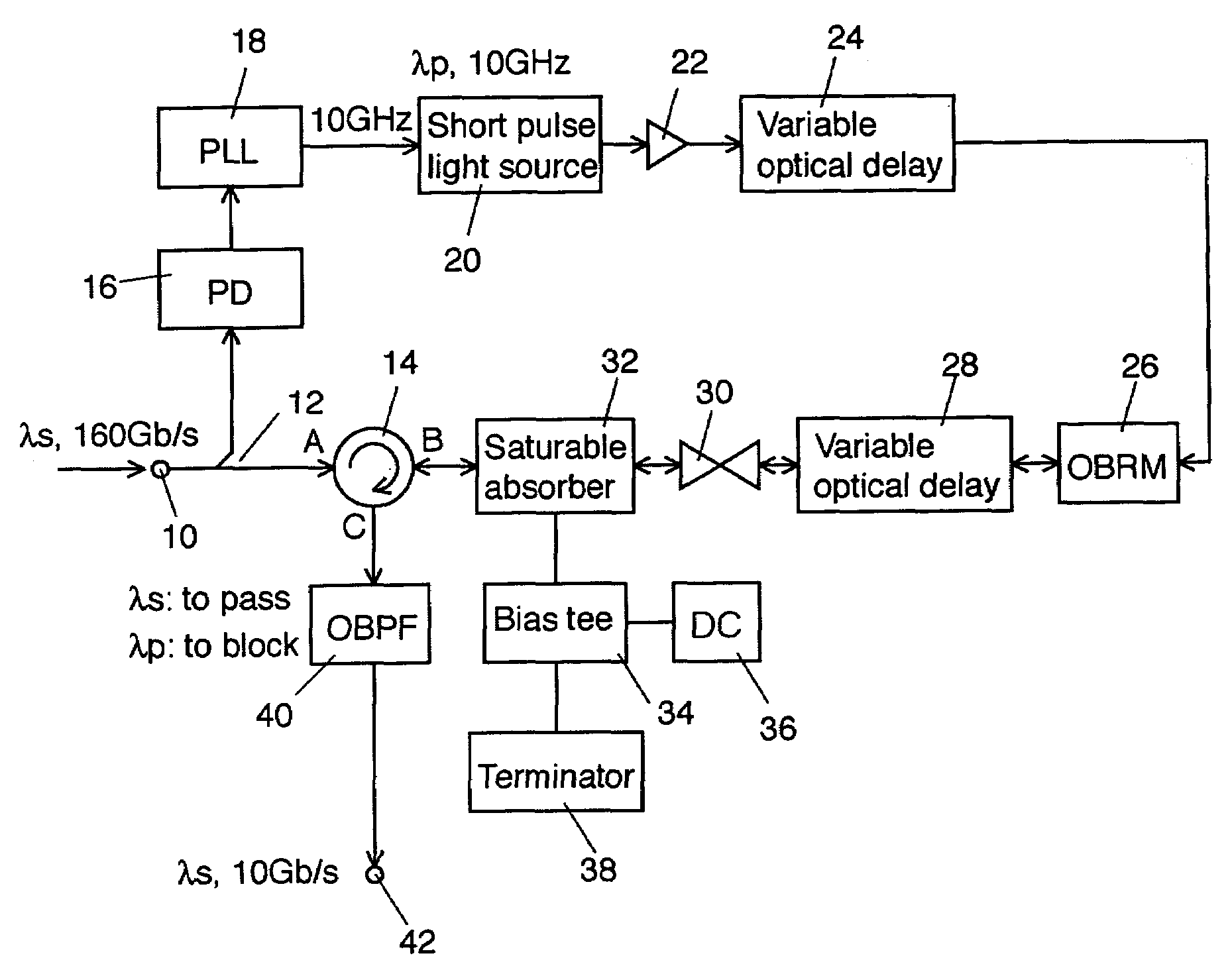
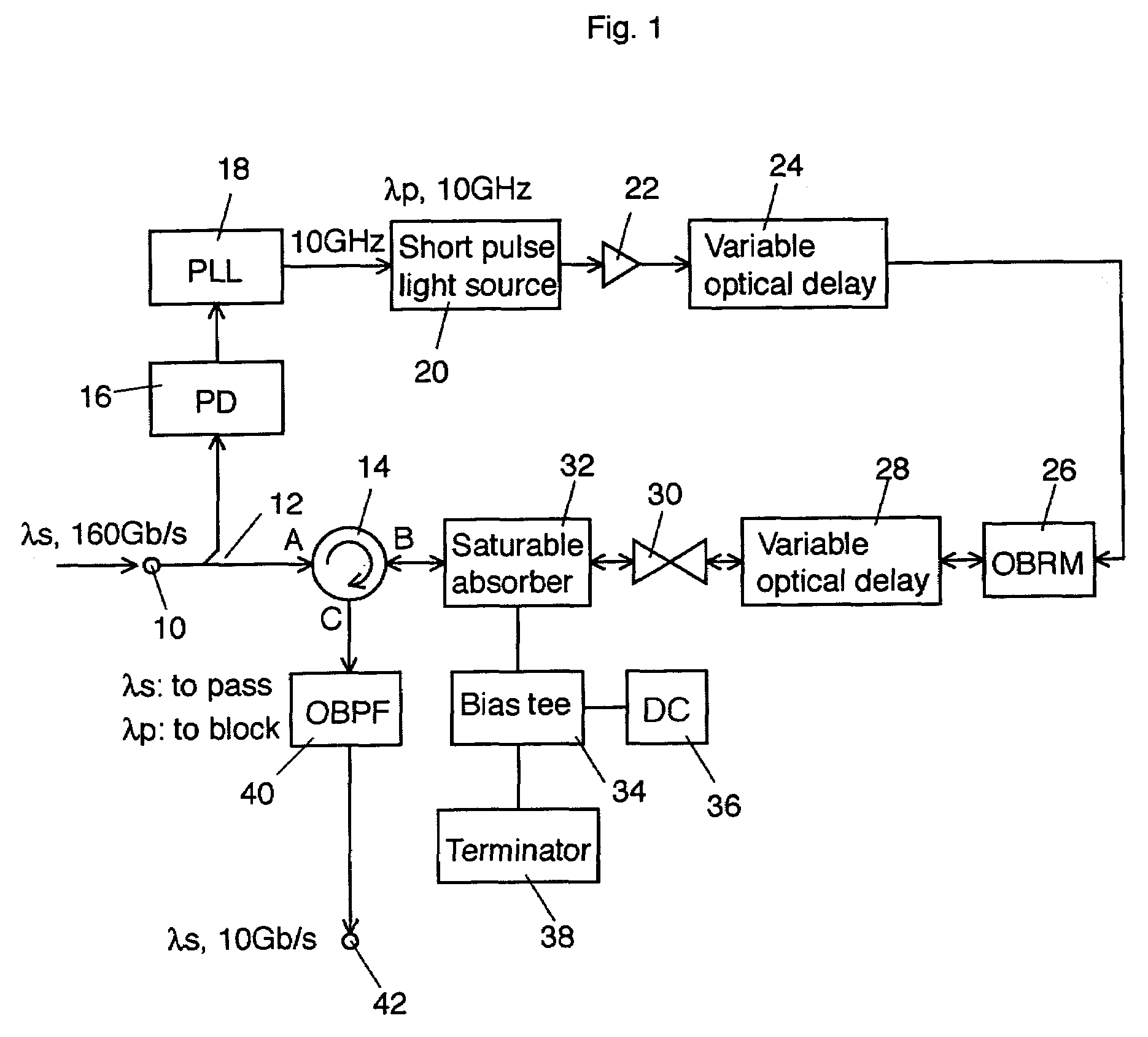
[0025]FIG. 1 is a schematic block diagram of a first explanatory embodiment according to the invention.

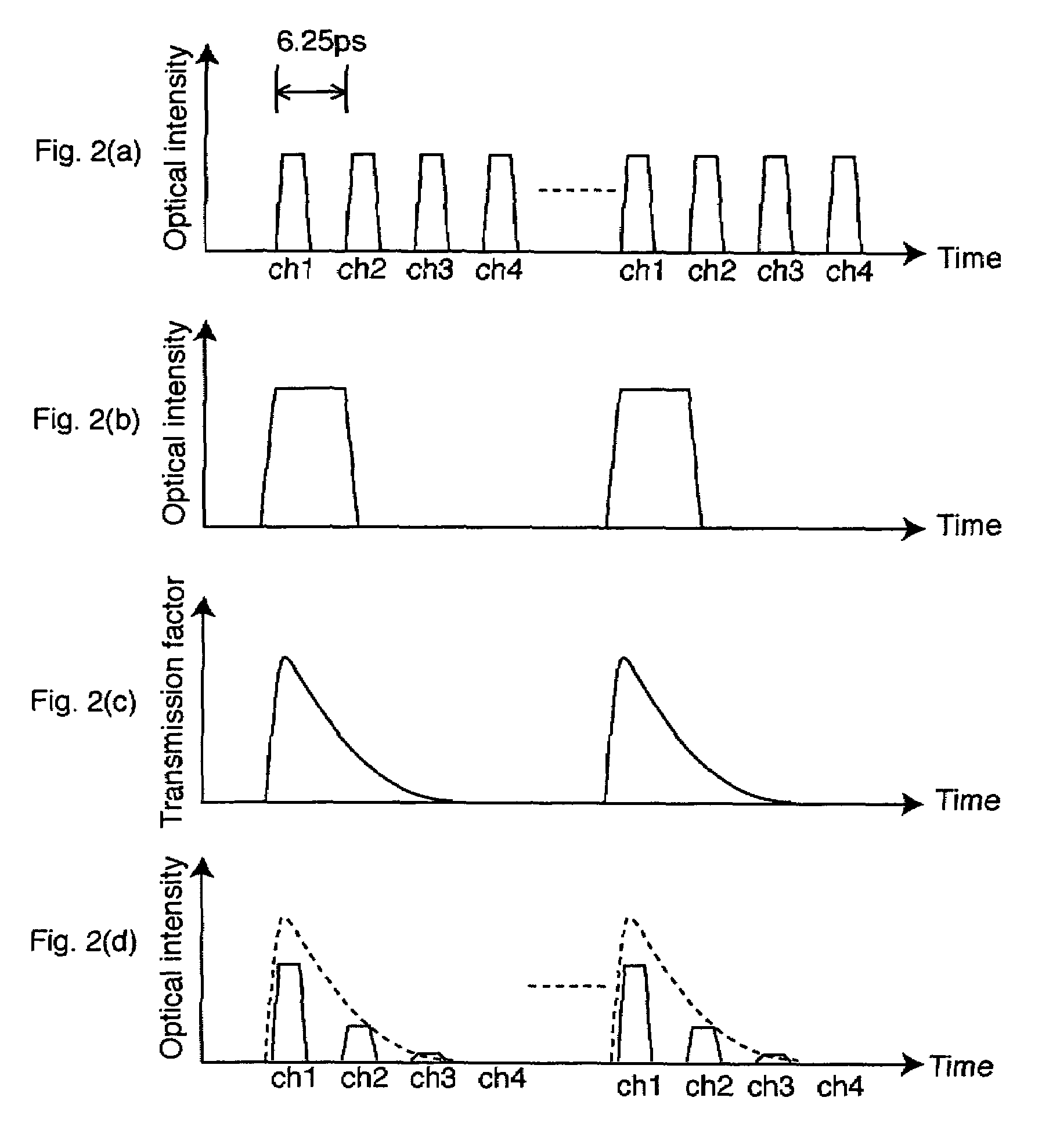
[0026]An optical pulse signal light having a signal wavelength λs at 160 Gbps enters an input terminal 10. Here, the optical pulse signal light at 160 Gbps comprises a signal light wherein 16 pulse data lights, namely 16 channels, at a base rate 10 Gbps are time-division-multiplexed. Amplitude of a pulse signal light of one channel is set slightly narrower than amplitudes of pulse signal lights of the other 15 channels, and by this configuration, a tone component at 10 GHz is superimposed on an optical pulse signal light at 160 Gbps. A tone component at 10 GHz also can be superimposed by modulating optical phase of the signal light instead of the amplitude. The width of each optical pulse of the optical pulse signal light at 160 Gbps is set to approximately 3 to 4 ps.

[0027]An...


PUM

PropertyMeasurementUnit
frequencyaaaaaaaaaa
signal wavelengthaaaaaaaaaa
frequencyaaaaaaaaaa

Abstract

To demultiplex a low-speed optical pulse signal from a high-speed optical pulse signal, an optical clock generator generates an optical clock of a control wavelength λp at a predetermined frequency out of a pulse signal light of a signal wavelength λs. On one side of a saturable absorber, an optical band reflection mirror is disposed to reflect a light of the signal wavelength λs and to transmit a light of the control wavelength λp. A pulse signal light of the signal wavelength λs reciprocates in the saturable absorber. An optical pulse of the pulse signal light of the signal wavelength λs enters the saturable absorber almost simultaneously with different optical pulses of the optical clock on the ways of going and returning. The saturable absorber has a transmission factor relative to the signal wavelength λs. The transmission factor varies as the saturable absorber absorbs a light of the control wavelength λp.

Description

CROSS REFERENCE TO RELATED APPLICATIONS[0001]This application claims priority to Japanese Patent Application No. 2003-303977, filed Aug. 28, 2003, the entire contents of which are incorporated herein by reference.FIELD OF THE INVENTION[0002]This invention generally relates to an optical pulse demultiplexer and method thereof, and more specifically relates to an optical pulse demultiplexer and method thereof to demultiplex a low-speed optical pulse signal from an ultra high-speed optical pulse at 160 Gbps or more.BACKGROUND OF THE INVENTION[0003]An ultra high-speed optical pulse signal can be generated by time-division-multiplexing a plurality of optical pulse signals (tributary channels), each carrying a data at the same standard bit rate (a base rate). For instance, when the base rate is 10 Gbps and the multiplexed number is 16, an ultra high-speed optical pulse signal at 160 Gbps can be generated. In a case that an ultra high-speed optical pulse signal having a single wavelength i...

Claims


Application Information

Patent Timeline
Patent Type & Authority Patents(United States)
IPC IPC(8): H04B10/00G02F1/01G02F1/015H01S3/091H01S3/092H01S3/113H04B10/524H04B10/54H04B10/556H04B10/58H04J14/08H04L7/00
CPCH04B10/299H04J14/08H04L7/0075
Inventor MIYAZAKI, TETSUYA
Owner NAT INST OF INFORMATION & COMM TECH
Why Eureka
Try Eureka